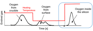
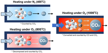
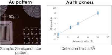
Semiconductors are the key evolving components in the industry today. HORIBA has kept its sights keenly focused on this micro world. Specialists in each field; We have pursued proprietary engineering projects in a wide range of areas that include evaluation and analysis, purity of ultra-pure water, composition of liquids and gases, and more broadly, environmental and safety. With our sights set clearly on the overall process, we have developed a line-up of analytical equipment, fluid control and measuring systems tailored to every stage of the semiconductor manufacturing process in response to stringent quality control requirements. In all stages, from materials evaluation through to final inspection, Our products help maintain high efficiency in the manufacture of leading-edge electronics devices.
Máte nějaké dotazy nebo požadavky? Pomocí tohoto formuláře kontaktujte naše specialisty.