
Real Time Interferometric Process Monitor LEM-CT-670-G50


Overview
Real Time Interferometric Process Monitor provides high precision detection of film thickness and trench depth during the etching/coating process.
Interference occurs when monochromatic light hits the sample surface, resulting in different optical path lengths due to film thickness and height variations in the film.
The system calculates the etching and coating speed of the monitored area by using time monitoring of the interference intensity based on the cycle, leading to detection of the end-point from the prescribed film thickness and trench depth.
Based on this relatively simple theory, the system is extremely stable and can be used with complex multi-layer films.
Features
Two types of lasers are available and compatible with a broad range of films including SiN, SiO2, GaAs, InP, AlGaAs, and GaN.
The system consists of a compact interference measurement section that includes the laser source, light receiver, and optical components, as well as the illumination and CCD imaging camera, allowing monitoring of any area of the wafer surface using microscopic images. This system uses a visible laser (670 nm) which can be used for a broad range of films.
Sensor head
- Camera with CCD imaging
A large objective lens to wafer distance attachment range of 200 mm to 800 mm. The use of lasers enables a spot diameter as small as 20 mm to 100 mm. A compact, self-contained amplifier design that allows simple monitoring of 0 V to 10 V outputs with only a camera if connected to devices such as a data logger.
- Traditional interference wave type
The horizontal axes represents time. An interference cycle is generated with respect to the etching depth as the etching process progresses. The amount of etching during one cycle is displayed as Dp = λ (laser wavelength 670 nm) / 2n (refractive index of etching film).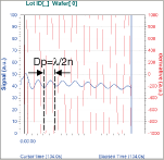
Software ready for built-in use in processing lines
This is a system for achieving high yield rates with semiconductors. Statistical processing from batch database compilation, remote control I/O common with the Semiconductor Manufacturing Process Monitor, and a remote control board for serial control from SECSII are included as standard features.
End-point detection algorithms with improved flexibility
With HORIBA JOBIN YVON’s own alarm expansion settings feature, a large number of compatible algorithms for special signal detection and detection of signals with poor S/N ratios are included and can always be expanded.
Advanced reprocessing features
Data obtained once can be simulated a number of times to achieve the optimum parameter configuration. This data can also be sent directly to HORIBA for analysis and optimization.
![]()
Manufactured by HORIBA
Specifications
Light source | Laser diode | |
|---|---|---|
Light source wavelength | 670 nm | |
Magnification | 50x (G50) | |
Spot diameter | 20 μm to 100 μm | |
Detector | Pin-photo diode | |
Camera | Dimensions | 65 (W) × 160 (H) × 100 (D) mm |
Mass | 1.2 kg, 2.6 lb | |
Controller | Dimensions | 451 (W) × 400 (H) × 133 (D) mm |
Mass | 10 kg, 22 lb | |
Stage specifications
Manual X-Y stage | ストローク:±8.0mm | |
|---|---|---|
Motor X-Y stage | ストローク:±12.5mm | |
Stage | Manual | 120 (W) × 120 (H) × 87 (D) mm |
Motor | 185 (W) × 102 (H) × 185 (D) mm | |
Options
Motor X-Y stage, pattern recognition device
Controller
Memory 256 MB, CPU 600 Mhz or greater, RAM 64 MB or greater, HDD 30 GB or greater
Attachment conditions
A measurement view port of ø20 or greater will be required in a vertical direction across the wafer.