
Real Time Interferometric Process Monitor DIGILEM-CPM-Xe/Halogen


Overview
Real Time Interferometric Process Monitor provides high precision detection of film thickness and trench depth during the etching/coating process.
Interference occurs when monochromatic light hits the sample surface, resulting in different optical path lengths due to film thickness and height variations in the film.
The system calculates the etching and coating speed of the monitored area by using time monitoring of the interference intensity based on the cycle, leading to detection of the end-point from the prescribed film thickness and trench depth.
Based on this relatively simple theory, the system is extremely stable and can be used with complex multi-layer films.
Features
Perfect for monitoring thin and highly transparent films such as GaN, AlGaN, SiO2, and SiN.
The newly developed (patent pending) ultraviolet sensor head allows the device to be used for monitoring thin and highly transparent films. Variation in refractive index with this laser wavelength is small, which means films that could not be measured because of a lack of reflection can now be measured using the interference method, by selecting an arbitrary wavelength from the internal spectrometer.
Plasma spectrographic analysis is also possible
The DIGILEM-CPM type has an internal spectrometer which means emission spectral analysis and measurement of end-points is now possible in addition to interference measurements. A high performance spectrometer and waveform processing software means the system is compatible with weak optical signals with a poor S/N ratio.
Sensor head
- UV light interference: TILT HEAD
A shorter distance between the objective lens and wafer means the diameter of the spot can be decreased, so a long neck design has been used. This has been installed near the high cycle antenna, while the body of the main lens does not contain any metal parts.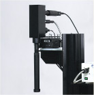
Software ready for built-in use in processing lines
This is a system for achieving high yield rates with semiconductors. Statistical processing from batch database compilation, remote control I/O common with the Semiconductor Manufacturing Process Monitor, and a remote control board for serial control from SECSII are included as standard features.
End-point detection algorithms with improved flexibility
With HORIBA JOBIN YVON’s own alarm expansion settings feature, a large number of compatible algorithms for special signal detection and detection of signals with poor S/N ratios are included and can always be expanded.
Advanced reprocessing features
Data obtained once can be simulated a number of times to achieve the optimum parameter configuration. This data can also be sent directly to HORIBA for analysis and optimization.
![]()

Laser device etching monitor screen
![]()
An example of a complete system using a pattern recognition device.
(The photo is the combination with the DIGILEM-CPM-Xe).
Manufactured by HORIBA
Specifications
Light source | Xe-Hg lamp / Halogen lamp | ||
|---|---|---|---|
Spot diameter | 100 to 500 μm | ||
Light source | Xe-Hg spectral line: 300 to 450 nm | ||
Magnification | 63x at 15" monitor | ||
Spectrometer | Resolution > 2.0 nm (with a 50 μm slit) | ||
Detector | CPM: 2048 Ch CCD detector | ||
Optical fiber | 2 branch fiber ultraviolet, visibility 5 m | ||
Controller | Dimensions | 220 (W) × 130 (H) × 400 (D) mm | |
Mass | 11 kg, 24.2 lb | ||
Stage specifications
Manual X-Y stage | ストローク:±8.0mm | |
|---|---|---|
Motor X-Y stage | ストローク:±12.5mm | |
Stage | Manual | 120 (W) × 120 (H) × 87 (D) mm |
Motor | 185 (W) × 102 (H) × 185 (D) mm | |
Options
Motor X-Y stage, pattern recognition device
Controller
Memory 256 MB, CPU 600 Mhz or greater, RAM 64 MB or greater, HDD 30 GB or greater
Attachment conditions
A measurement view port of ø20 or greater will be required in a vertical direction across the wafer.