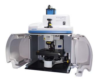
SmartSPM Scanner and Base
Sample scanning range: 100 µm x 100 µm x 15 µm (±10 %)
Scanning type by sample: XY non-linearity 0.05 %; Z non-linearity 0.05 %
Noise: 0.1 nm RMS in XY dimension in 200 Hz bandwidth with capacitance sensors on; 0.02 nm RMS in XY dimension in 100 Hz bandwidth with capacitance sensors off; < 0.04 nm RMS Z capacitance sensor in 1000 Hz bandwidth
Resonance frequency: XY: 7 kHz (unloaded); Z: 15 kHz (unloaded)
X, Y, Z movement: Digital closed loop control for X, Y, Z axes; Motorized Z approach range 18 mm
Sample size: Maximum 40 x 50 mm, 15 mm thickness
Sample positioning: Motorized sample positioning range 5 x 5 mm
Positioning resolution: 1 µm
AFM Head
Laser wavelength: 1300 nm, non-interfering with spectroscopic detector
Registration system noise: Down to < 0.1 nm
Alignment: Fully automated cantilever and photodiode alignment
Probe access: Free access to the probe for additional external manipulators and probes
SPM Measuring Modes
Contact AFM in air/(liquid optional); Semicontact AFM in air/(liquid optional); Non -contact AFM; Phase imaging; Lateral Force Microscopy (LFM); Force Modulation; Conductive AFM (optional); Magnetic Force Microscopy (MFM); Kelvin Probe (Surface Potential Microscopy, SKM, KPFM); Capacitance and Electric Force Microscopy (EFM); Force curve measurement; Piezo Response Force Microscopy (PFM); Nanolithography; Nanomanipulation; STM (optional); Photocurrent Mapping (optional); Volt-ampere characteristic measurements (optional)
Spectroscopy Modes
Confocal Raman, Fluorescence and Photoluminescence imaging and spectroscopy
Tip-Enhanced Raman Spectroscopy (TERS) in AFM, STM, and shear force modes
Tip-EnhancedPhotoluminescence (TEPL)
Near-field Optical Scanning Microscopy and Spectroscopy (NSOM/SNOM)
Conductive AFM Unit (optional)
Current range: 100 fA ÷ 10 µA; 3 current ranges (1 nA, 100 nA and 10 µA) switchable from the software
Optical Access
Capability to use simultaneously top and side plan apochromat objective: Up to 100x, NA = 0.7 from top or side; Up to 20x and 100x simultaneously
Closed loop piezo objective scanner for ultra stable long term spectroscopic laser alignment: Range 20 µm x 20 µm x 15 µm; Resolution: 1 nm
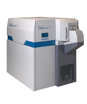
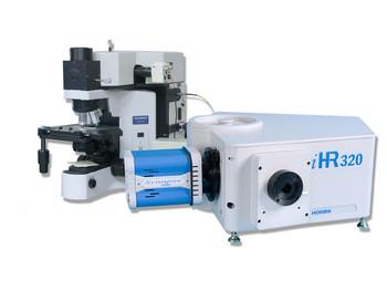
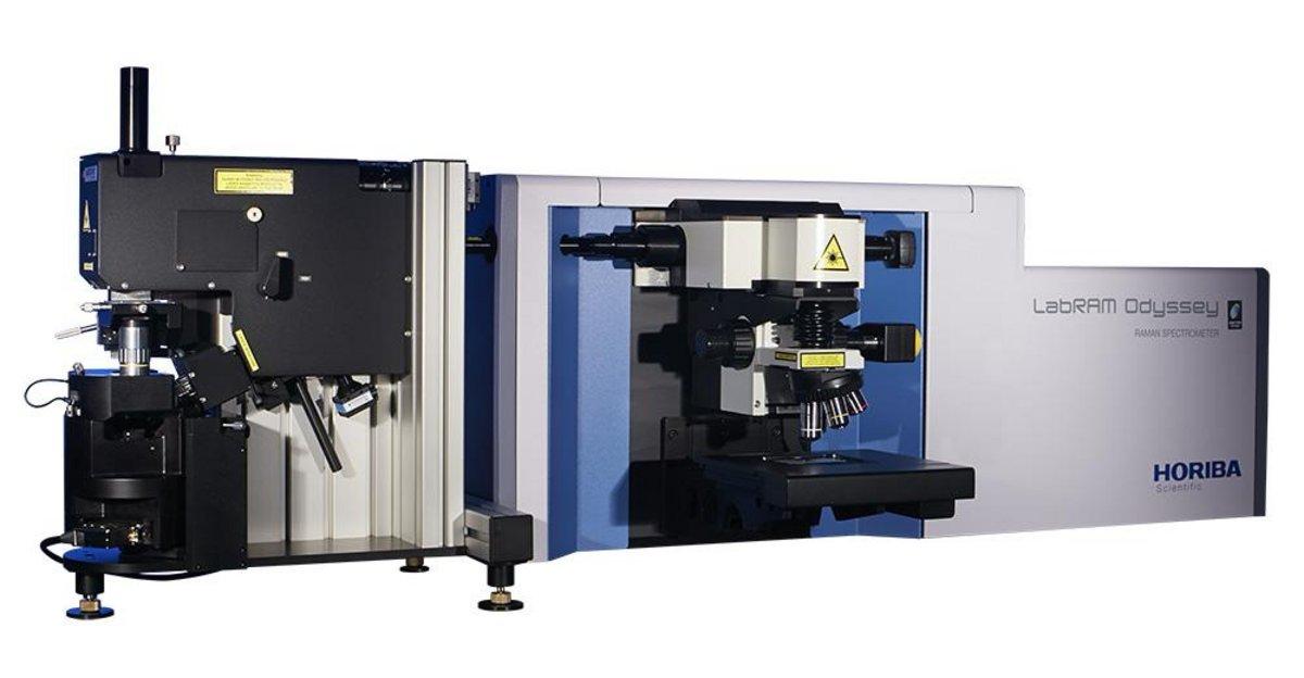
Spectrometer
Fully automated high resolution LabRAM Odyssey micro-spectrometer, functional as stand-alone micro-Raman microscope
Wavelength range: 50 cm-1 to 4000 cm-1 or down to 10 cm-1 with Ultra Low Frequency (ULF) filter option
Gratings: Selection of gratings from 150 g/mm to 3600 g/mm; 2 gratings on computer controlled turret, kinematically mounted and easily exchangeable
Optical design: Achromatic spectrograph and achromatic coupling optics
Automation: Fully motorized, software controlled operation
Detection
Full range of CCD detectors and EMCCDs and InfraRed detectors: InGaAs array, single channel extended InGaAs, InSb, CdTe,...
Laser Sources
Wavelengths: Full range of wavelengths from DUV (229 nm) to IR (up to 1064 nm)
Typical wavelength: 532 nm, 638 nm, 785 nm
Automation: Fully automated laser and filter switching for up to 3 simultaneous lasers; Laser polarization selection and spectral analyzer options for all wavelengths
Software
Integrated software package including full featured SPM, spectrometer and data acquisition control, spectroscopic and SPM data analysis and processing suite, including spectral fitting, deconvolution and filtering, optional modules include univariate and multivariate analysis suite (PCA, MCR, HCA, DCA), particle detection and spectral search functionalities.


")