
Raman-PL Systems


Overview
HORIBA Scientific offers unique Raman-Photoluminescence configurations for the LabRAM HR and LabRAM ARAMIS systems.
These Raman-PL mapping systems are used in production environments to provide key information on epitaxy layer crystal quality, composition and homogeneity across full wafers. Such systems are also used for research oriented tasks such as measuring photoluminescence images of devices and nano-materials.
Features
Multiple detectors
Emission spectra in photoluminescence (PL) measurements often extend out beyond 1.1 µm in the near infra-red (NIR), where conventional Raman instruments using CCD detectors are usually not sensitive. To achieve combined Raman and photoluminescence analysis, the LabRAM Raman-PL systems include two ports for different detectors - a standard Raman CCD detector and InGaAs array detector, the latter being ideally suited to the NIR PL range. As an option, a third single channel detector can also be incorporated, allowing analysis still further into the NIR.
The unique optical design and dual detector options of the Raman-PL systems provides easy operation across the broadest spectral range - no changing of internal optics, no re-alignment of achromats and no loss in performance. The CCD detector range is optimized for the important Raman measurements, whilst the IR array detector options open up access to the NIR PL range, an important new factor for the comprehensive material characterization. The user has the ability to switch between Raman and PL analysis without any need for adjustment. The instruments combine the two techniques and enable both measurements to be made at exactly the same position on the sample for precise characterization and analysis.
|
|
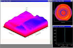
PL intensity map and histogram of a semiconductor wafer | Thermal donor characterisation of a silicon wafer based on infra-red PL mapping. |

High spectral resolution
The unique long focal length spectrometers of the Raman-PL systems allows access to true high spectral resolution measurements, in addition to standard low-medium resolution analysis. Spectral resolution down to 0.3-0.4 cm-1 (~0.01nm) is routinely achievable, depending on the system and configuration.
High spectral resolution is ideally suited for the analysis of subtle spectral changes, including the investigation of semiconductor stress/strain and material crystallinity.
Dedicated PL software
A dedicated photoluminescence software module is available. It provides specific PL analysis and acquisition features ideally matched to the requirements of the semiconductor industry.
Click here for more information about LabSpec Raman-PL software
Manufactured by HORIBA Scientific