


拉曼研究解决方案

从高性能共聚焦拉曼光谱到定制的解决方案,我们自1968年以来一直支持研究工作!
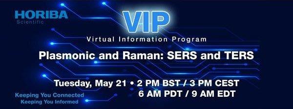
Raman spectroscopy is a good technique for chemical and physical characterization of materials, but suffers from a few limitations like a lack of sensitivity, or its micron scale resolution. Since the 1970s, the coupling of the plasmonic effect with Raman is more and more being used to overcome these limits. This phenomena association results in two enhanced Raman spectroscopies called SERS and TERS, respectively associated to Surface and Tip origins.
During this webinar, we will present how the coupling of plasmonic and Raman effects results to with SERS and TERS and details some applications.
Microplastics are becoming the 21st century environmental scourge. To control it, more and more regulations are being set in all countries worldwide to monitor the amount of microparticles released in the environment. Thus, some techniques have been identified as reference methods: Pyrolysis GC-MS, Infrared microscopy, and Raman microscopy. This last one provides the best combination of information in both morphological and chemical characterization of each particle down to the micron.
During this webinar, we will present how Raman microscopy is becoming the best reference method for microplastics characterization.
With the global energetic transition and the move from thermic to electric cars, the improvement of battery becomes crucial. With that development, the analytical techniques used must be also adapted and developed to understand the physical and chemical processes occurring at the electrodes and electrolyte levels. Thus, Raman microscopy is an ideal method as it provides physical and chemical properties of materials in a non-invasive approach.
During this webinar, we will present how Raman microscopy can be applied for battery characterization, and for fuel cells, the future of batteries.
Watch it nowRaman microscopy is the combination of the Raman effect and optical microscopy. A Raman microscope is the association of multiple components where each of them is playing a specific role to achieve highly resolved and sensitive measurements.
During this webinar, we will present the role of each component of a Raman microscope and detail their characteristics and limits.
Particulate matter poses a growing threat to air quality and public health. To effectively understand the effects and assess the hazardousness of particles, it is necessary to study them on a molecular level. Raman spectroscopy emerges as an effective method for revealing the chemical composition of airborne particles at the microscopic scale.
This Raman XPerience article reviews a selection of user's papers on this topic.
Read moreSubscribe to our newsletter and receive updates on products, software, applications, Tips & Tricks videos, and service.
Subscribe由于Covid-19的出现,现在市场上出现了多种多样的防护口罩。这些类型的口罩尤其因其与过滤能力有关的不同效率而有所区别。因此,这些保护性的差异使得对口罩的成分研究变得非常重要。因此,防护性能上的这些差异使得口罩的纤维成分变得至关重要。在本文中,我们介绍了为什么LabRAM Soleil™ 共聚焦拉曼是研究口罩的纤维分布和组成的理想工具。
查看详情由于Covid-19的出现,现在市场上出现了多种多样的防护口罩。这些类型的口罩尤其因其与过滤能力有关的不同效率而有所区别。因此,这些保护性的差异使得对口罩的成分研究变得非常重要。因此,防护性能上的这些差异使得口罩的纤维成分变得至关重要。在本文中,我们介绍了为什么LabRAM Soleil™ 共聚焦拉曼是研究口罩的纤维分布和组成的理想工具。
查看详情由于Covid-19的出现,现在市场上出现了多种多样的防护口罩。这些类型的口罩尤其因其与过滤能力有关的不同效率而有所区别。因此,这些保护性的差异使得对口罩的成分研究变得非常重要。因此,防护性能上的这些差异使得口罩的纤维成分变得至关重要。在本文中,我们介绍了为什么LabRAM Soleil™ 共聚焦拉曼是研究口罩的纤维分布和组成的理想工具。
查看详情由于Covid-19的出现,现在市场上出现了多种多样的防护口罩。这些类型的口罩尤其因其与过滤能力有关的不同效率而有所区别。因此,这些保护性的差异使得对口罩的成分研究变得非常重要。因此,防护性能上的这些差异使得口罩的纤维成分变得至关重要。在本文中,我们介绍了为什么LabRAM Soleil™ 共聚焦拉曼是研究口罩的纤维分布和组成的理想工具。
查看详情在本网络研讨会中,将介绍与颗粒相关拉曼光谱(PCRS)技术,并涉及医学、制药/化妆品和微小颗粒等领域的代表性应用实例加以说明,包括对各种类型的样品(包括粉末、片剂和悬浮液)的处理和制备的讨论。
在本网络研讨会中,将介绍与颗粒相关拉曼光谱(PCRS)技术,并涉及医学、制药/化妆品和微小颗粒等领域的代表性应用实例加以说明,包括对各种类型的样品(包括粉末、片剂和悬浮液)的处理和制备的讨论。
查看详情高分辨超灵敏智能拉曼成像仪
高性能全自动拉曼光谱
纳米拉曼光谱仪
台式拉曼光谱仪
多功能拉曼及成像光谱仪
纳米拉曼光谱仪
台式大光路拉曼光谱仪
先进原子力显微镜
Photoluminescence and Raman Wafer Imaging
光谱仪
多光路耦合纳米拉曼光谱仪
高速高分辨显微共焦拉曼光谱仪
生物型纳米拉曼光谱仪
AFM光学工作站
用于紫外拉曼光谱学家
坚固耐用的科研级便携拉曼光谱仪
如您有任何疑问,请在此留下详细需求信息,我们将竭诚为您服务。