Browse Products

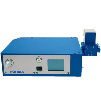
MicOS
Photoluminescence Microspectrometer

LabRAM Odyssey Semiconductor
Photoluminescence and Raman Wafer Imaging

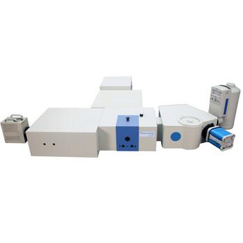
FluoroMax Plus
Steady State and Lifetime Benchtop Spectrofluorometer
Modular TeraHertz Raman Spectrometer
Affordable ultra-low frequency Raman spectrometer down to 10 cm-1

LabRAM HR Evolution
Confocal Raman Microscope
Nanolog
Steady State and Lifetime Nanotechnology EEM Spectrofluorometer
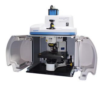
XploRA™ PLUS
Raman Spectrometer - Confocal Raman Microscope

LabRAM Odyssey
Confocal Raman Imaging & High Resolution Spectrometer

EasyLife L
Phosphorescence Lifetime Spectrometer
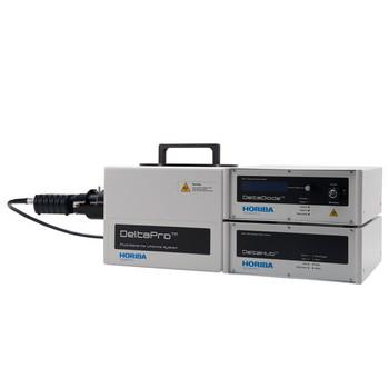
DeltaPro
TCSPC Lifetime Fluorometer

Duetta
Fluorescence and Absorbance Spectrometer
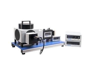
DeltaFlex
TCSPC/MCS Fluorescence Lifetime System

EasyLife X
Lifetime Fluorescence Spectrometer