Process Control and In-situ Measurement for Photovoltaic Manufacturing Process


Endpoint / Chamber Health Monitor based on Optical Emission Spectroscopy and MWL Interferometry
To address new requirements in Semiconductor, lighting devices, automotive components, flat panels, MEMS sensors, memory chips, and logic electronics processed in the industry using dry etch, cleaning and (PE)CVD, HORIBA has introduced a unique generation of sensor dedicated to Advanced Endpoint Control, Fault Detection and Chamber Health Monitoring.
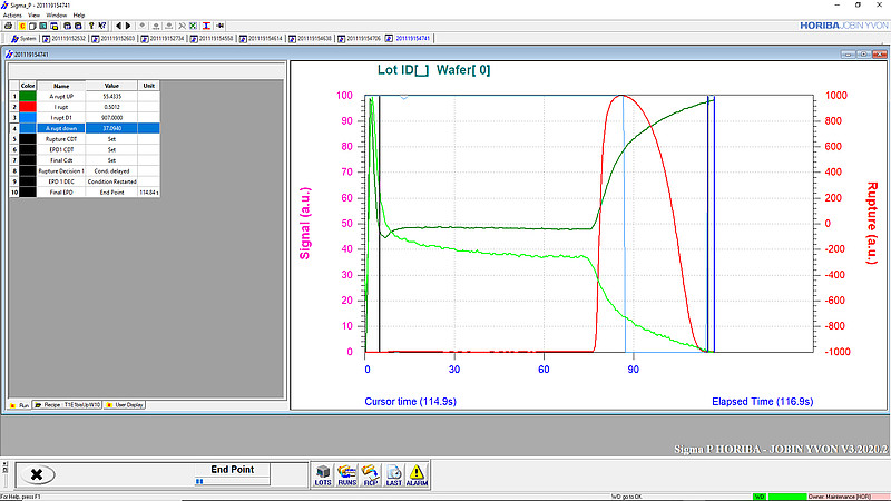
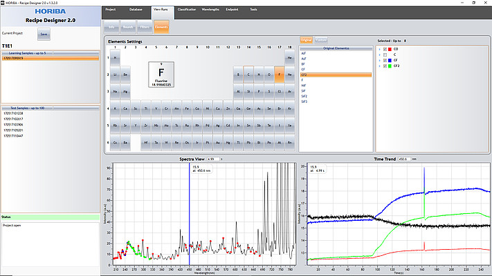
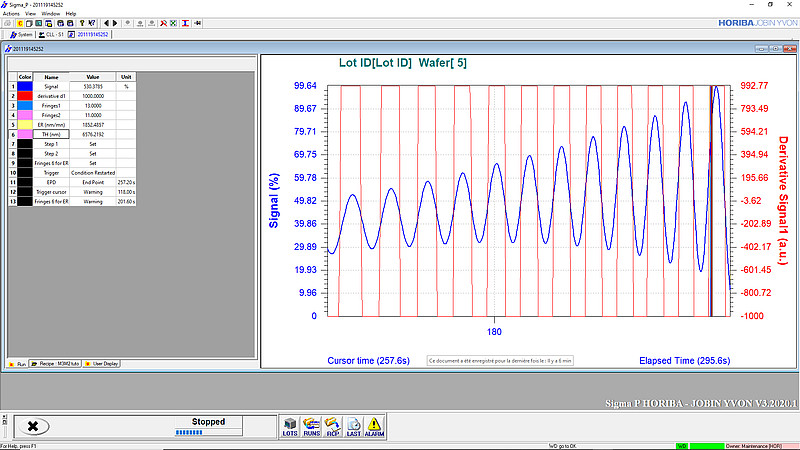
EV 2.0 is a configurable high-performance spectrograph, customized for a variety of semiconductor OEMs and end-user applications, including Process Engineering with automatic Endpoint Recipe creation, and on-board processing performing full endpoint and process quality management
Depending on accessories, EV 2.0 is dedicated to Optical Emission Spectroscopy (OES) or Multiwavelength Interferometry (INT) Endpoint process real-time Monitoring, on single chamber or cluster tool configuration.
EV 2.0 belongs to EV actual family to introduce modularity. EV 2.0 is ideal for monitoring in-situ the health of plasma, process stability, leaks, arcing and abnormal plasma behavior as well as detecting the endpoint in OES or INT configuration.


Generality
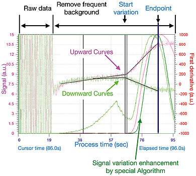
Regarding CCD based OES (Optical Emission Spectroscopy) or Interferometry (Laser or Multiwavelength using broad Flash Lamp source), endpoint detection mostly consists in three steps:
To address these new requirements, HORIBA has developed a unique generation of Sensor (Hardware and Software), based on OES and/or interferometry, for Endpoint, fault detection, Chamber health monitoring and Advanced Process Control (APC) adaptable to all etchers, to help engineers and Fab’s to manage actual and future products and technologies.
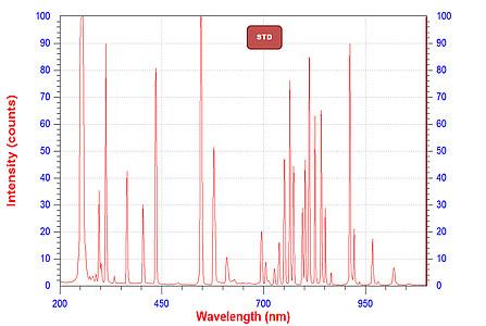
Optical Emission Spectroscopy: OES
EV 2.0 to take full advantage of the OES wealth
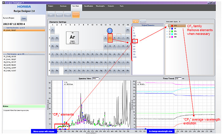
EV 2.0, using Optical Emission Spectroscopy (OES), allows the study of spectra emitted by atoms and ions with optical transition in the UV-VIS-NIR regions. OES, as a rich qualitative tool, is the only mean for process engineers, without any intrusive plasma perturbation:
With EV 2.0, Horiba offers a versatile solution from R&D to industrial applications for:
Interferometry: INT
EV 2.0 INT for Real-Time accurate and reliable Thickness/depth information
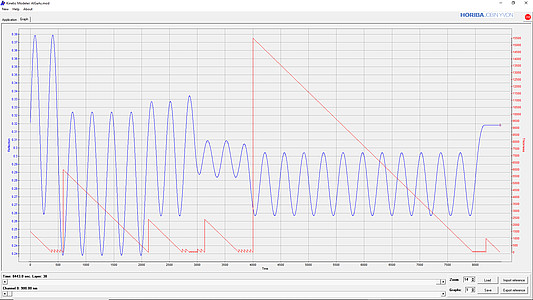
Besides plasma, Sample information is also complex. EV 2.0 INT (as LEM-CT), mounted on any process chamber with direct top view of the wafer,allows to obtain local information on optically semi-transparent, multi-layers structure. This allows the etch rate and thus etched thickness to be monitored in real time, providing enhanced process control for a wide variety of processes. Additionally, interfaces can be detected by their change in reflectivity.
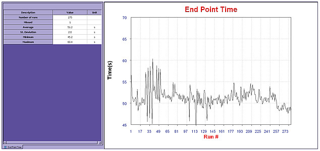
Based on the interferometry technique, EV 2.0 INT is ideally suited to etch/deposition rate monitoring and endpoint detection, providing high precision detection of Fringes counting, film thickness, trench depth, interfaces…
| System outline | The small sized spectrometer is based on a concave holographic grating (aberration corrected) with 20mm focal length (LR) or 75 mm focal length (STD, HR) and 50µm slit. The spectrometer is attached to a window of the Tool chamber or through SMA fiber. 3 models of spectrometers:
| ||||||
|---|---|---|---|---|---|---|---|
| Grating | HORIBA Aberration corrected Concave grating | ||||||
| Detector | BT CCD Maker: Hamamatsu Photonics | ||||||
| Electronics | BT CCD Electronics Maker: HORIBA, Ltd. Model: JY70 16bit acquisition electronic Exposure time: 1 ms ~ 10 sec The following ports are installed 1. LAN Ethernet 100Mbps RJ45 (TCP/IP) 2. IOR 70 Remote Db25 PIO-RS 3. DC Power supply: 9 to 24V, Standard 24V | ||||||
| Spectrometer LR | Model: EV2.0 LR (Low Resolution)
| ||||||
| Spectrometer STD | Model: EV2.0 STD (Standard Resolution)
 | ||||||
| Spectrometer HR | Model: EV2.0 HR (High Resolution)
| ||||||
| Remote | EV 2.0 may be connected to any host through digital Link with RJ 45 connector: TCP/IP.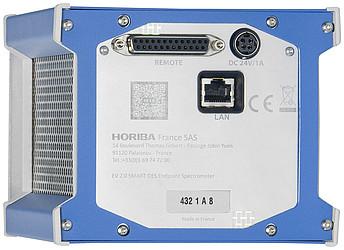 EV 2.0 spectrometer contains an interface board to provide galvanic isolation between the host controller hardware of the HOST / Tool from the spectrometer main electronics.
| ||||||
| Certification | CE | ||||||
| Integration | 3U integration or stand alone with HORIBA Blue cover |
| DC Power Supply | 24V |
|---|---|
| SSD | 256 Go, 2,5” SATAIII |
| Design | Aluminum Frame, fanless design Anti-vibration and shock resistant |
| Connection | RS-232/422/485 RS-232 USB 3.0 on Standard 2x RJ45 Gb VGA, HDMI … |
| Standard PC (Default) | |
|---|---|
| CPU | 64bits, Intel® Pentium® N4200, 2.5 GHz |
| RAM | 4Go DDR3 |
| Controller Dimensions | 197 (W) x 110 (D) x 55 (H) mm |
| Controller Mass | 2 kg |
| High Grade PC (Optional) | |
|---|---|
| CPU | 64bits, Intel® Core™ i7-7700T 2,9 GHz |
| RAM | 8Go DDR4 2133MHz |
| Controller Dimensions | 264 (W) x 96.4 (D) x 186.2 (H) mm |
| Controller Mass | 4.5 kg |
| Accessories for Optical Emission Spectroscopy (Chamber side window) |
|
|---|---|
| Accessories for Interferometry (Chamber top window) |
|
| Accessories for Spectrometer and PC |
|
| Software | 3 choices of software
|
| Various Configurations |
|
| Operating Temp/humidity | Temp:18℃~50℃ Humidity:0~70%RH (No dew condensation) |
|---|---|
| Transportation Temp/humidity | Temp:-20℃~55℃ Humidity:0~70%RH (No dew condensation) |
Tiene alguna pregunta o solicitud? Utilice este formulario para ponerse en contacto con nuestros especialistas.
Exhaust Pressure Controller
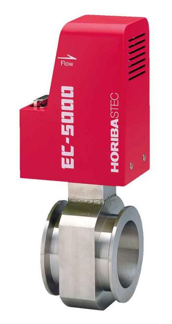
Optical Emission Spectroscopy Etching End-point Monitor
Digital Liquid Mass Flow Meters / Controllers
Compact Baking System
Liquid Auto Refill System
Mixed Injection System Liquid Vaporizers
Mixed Injection System Liquid Vaporizer
Piezo Actuator Valve
High Temperature Digital Mass Flow Controller
Digital Mass Flow Controller
Multi Range/Multi Gas Digital Mass Flow Controller
Digital Automatic Pressure Regulator
Direct Liquid Injection System

Optical Emission Spectroscopy Etching End-point Monitor
Optical Emission Spectroscopy Etching End-point Monitor
Discover a Whole New World of Information with Glow Discharge Optical Emission Spectrometer
Plasma Emission Controller