LabRAM Soleil Nano

LabRAM Soleil Nano product image

Real-time and Direct Correlative Nanoscopy

Fully integrated system based on our OmegaScope scanning probe microscope and LabRAM Soleil Raman microscope. LabRAM Soleil Nano offers unprecedented capabilities for direct co-localized AFM-Raman and photoluminescence measurements. AFM imaging modes (topographic, electrical, mechanical, etc.) and Raman acquisition can be performed either sequentially or simultaneously at the same location of the sample surface. Optical nano-resolution is also achievable with Tip-Enhanced Raman Spectroscopy and Photoluminescence (TERS/ TEPL). LabRAM Soleil Nano is compatible with the environmental chamber for AFM and Raman measurements in controlled atmosphere and at low temperatures.

Segment: Scientific
Oddělení: AFM and AFM-Raman
Výrobní společnost: HORIBA France SAS

Multi-sample analysis platform

Macro, micro and nano scale measurements can be performed on the same AFM-Raman platform.

Multi-technique / Multi-environment

Numerous SPM (scanning probe microscopy) modes including AFM, force curves measurements, conductive and electrical modes (cAFM, KPFM), STM, liquid cell and electrochemical environment, together with chemical mapping through TERS/TEPL. Full control of the acquisition through one workstation and a powerful software control. SPM and Raman/PL microscope can be operated simultaneously or independently.

Compatible with the AFM chamber for environmental control, humidity control and cooling sample holder.

Robustness / Stability

High resonance frequency AFM scanners. High performance is obtained without active vibration isolation.

Ease-of-use

Fully automated operation, start measuring within minutes, not hours!

High collection efficiency

Top-down and oblique Raman/PL detection with high numerical aperture objectives for optimum resolution and throughput in both co-localized and tip-enhanced measurements (Raman and Photoluminescence).

High throughput multimodal UV-VIS-NIR achromatic platform

Designed for Raman, Photoluminescence, Electroluminescence and more.
Up to 4 internal lasers and 6 different filters; 4-grating turret.

High spatial resolution

Nanoscale spectroscopic resolution (down to 10 nm) through Tip-Enhanced Optical Spectroscopies (TERS: Tip-Enhanced Raman Spectroscopy, and TEP: Tip-Enhanced Photoluminescence).

Super-low cut-off frequency down to 30 cm-1 with high throughput

Ultrafast Raman imaging

SmartSampling™ - 100 times faster Raman maps - turns hours into minutes
3D Raman lightsheet confocal imaging with patented Q-Scan™

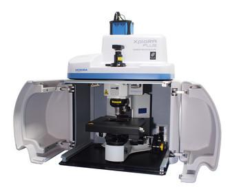
SmartSPM Scanner and Base

Sample scanning range: 100 µm x 100 µm x 15 µm (±10 %)

Scanning type by sample: XY non-linearity 0.05 %; Z non-linearity 0.05 %

Noise: 0.1 nm RMS in XY dimension in 200 Hz bandwidth with capacitance sensors on; 0.02 nm RMS in XY dimension in 100 Hz bandwidth with capacitance sensors off; < 0.04 nm RMS Z capacitance sensor in 1000 Hz bandwidth

Resonance frequency: XY: 7 kHz (unloaded); Z: 15 kHz (unloaded)

X, Y, Z movement: Digital closed loop control for X, Y, Z axes; Motorized Z approach range 18 mm

Sample size: Maximum 40 x 50 mm, 15 mm thickness

Sample positioning: Motorized sample positioning range 5 x 5 mm

Positioning resolution: 1 µm
 

AFM Head

Laser wavelength: 1300 nm, non-interfering with spectroscopic detector

Registration system noise: Down to < 0.1 nm

Alignment: Fully automated cantilever and photodiode alignment

Probe access: Free access to the probe for additional external manipulators and probes
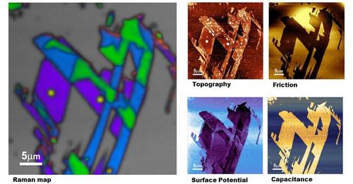
 

SPM Measuring Modes

Contact AFM in air/(liquid optional); Semicontact AFM in air/(liquid optional); Non -contact AFM; Phase imaging; Lateral Force Microscopy (LFM); Force Modulation; Conductive AFM (optional); Magnetic Force Microscopy (MFM); Kelvin Probe (Surface Potential Microscopy, SKM, KPFM); Capacitance and Electric Force Microscopy (EFM); Force curve measurement; Piezo Response Force Microscopy (PFM); Nanolithography; Nanomanipulation; STM (optional); Photocurrent Mapping (optional); Volt-ampere characteristic measurements (optional)
 

Spectroscopy Modes

Confocal Raman, Fluorescence and Photoluminescence imaging and spectroscopy

Tip-Enhanced Raman Spectroscopy (TERS) & Tip-Enhanced Photoluminescence (TEPL)  in AFM, STM, and shear force modes

Near-field Optical Scanning Microscopy and Spectroscopy (NSOM/SNOM)
 

Options

  • Conductive Unit: Current range 100fA ÷ 10uA / 3 current ranges (1nA, 100nA and 10 µA) switchable from the software
  • Liquid Cell / Electrochemical Cell
  • Temperature control for liquid cell: Heating up to 60°C
  • Environmental Chamber
  • Humidity control system: Relative humidity range 10-85% / Relative humidity stability ±1%
  • Heating Cooling module: From -50°C to +100°C
  • Heating module: heating up to 300°C / Temperature stability 0.1°C, or heating up to 150°C / Temperature stability 0.01°C
  • Combined Shear-force and Normal force tuning fork holder
  • STM holder
  • Signal Access Module


Optical Access

Capability to use simultaneously top and side plan apochromat objective: Up to 100x, NA = 0.7 from top or side; Up to 20x and 100x simultaneously

Closed loop piezo objective scanner for ultra stable long term spectroscopic laser alignment: Range 20 µm x 20 µm x 15 µm; Resolution: 1 nm
 

Spectrometer

Wavelength range: UV-VIS-NIR; Broadband high throughput achromatic mirror-based system, optimized from 300 nm to 1600 nm without changing optics.

Built-in lasers: Up to 4 Solid-state lasers, NUV to NIR wavelengths available.

External lasers: Unlimited, for large gas and ultrafast lasers typically.

Spectrometer scanning speed: Up to 400 nm/s, with 600g/mm grating, mounted on standard 4-grating turret.

Number of gratings: unlimited; 4-grating exchangeable motorized turret.

Fast Imaging: <1ms/spectrum  SWIFT, SWIFT XS EMCCD, SWIFT repetitive, SWIFT eXtended Range and SmartSampling for ultrafast imaging.

Standard wavenumber cut-off: 30 cm-1, with edge filters for 532, 638 and 785 nm wavelengths, injection rejection, >99% transmission.


Software

Integrated software package including full featured SPM, spectrometer and data acquisition control, spectroscopic and SPM data analysis and processing suite, including spectral fitting, deconvolution and filtering, optional modules include univariate and multivariate analysis suite (PCA, MCR, HCA, DCA), particle detection and spectral search functionalities.

TERS Characterization of Lipid Nanotubes as Carbonaceous Material for Electrodes
For thirty years there has been a research focused onto carbonization of 3D structures especially to be employed in electronic applications. These structures are prepared with the help of lithography and pyrolyzed afterwards. For making features below 100 nm, a bottom-up approach using lipids nanotubes is attempted.
TERS Characterization of Single- to Few-Layer Ti₃C₂Tₓ MXene
MXenes is the largest and fastest growing 2D materials. They have unique properties such as good conductivity and a hydrophilic surface. The control of nanoscale composition would ultimately allow for engineering properties locally, gaining more control over the 2D material-based systems.
TERS on Functionalized Gold Nanostructures for Nano-scale Biosensing
Surface-enhanced Raman scattering (SERS) is a powerful plasmonics-based analytical technique for biosensing. SERS effect relies on nanostructures that need to be designed to maximize enhancement factors and molecular specificity. In addition to numerical modeling, an analytical tool capable of imaging localized enhancement would be an added value.
TERS Characterization of phospholipid bilayers and detection of nanoparticles
Phospholipid bilayers, major constituents of membranes act as a barrier of selective permeability for the nanoparticles now largely into our environment. Studying the interactions between nanoparticles and cellular membranes requires a molecular chemical probe with nanometer resolution capability.
TERS Characterization of Explosive Nanoparticles
It is not yet understood how co-crystal nanoparticles (co-crystallinity combined with nanostructuring) have superior properties to single compound crystals. Only a technique capable of probing single nanoparticles can bring answers.
c-AFM and in operando TERS & µRaman Characterization of Molecular Switching in Organic Memristors
Emergence of organic memristors has been hindered by poor reproducibility, endurance stability scalability and low switching speed. Knowing the primary driving mechanism at the molecular scale will be the key to improve the robustness and reliability of such organic based devices.
Correlated TERS and KPFM of Graphene Oxide Flakes
Visualizing the distribution of structural defects and functional groups present on the surface of two-dimensional (2D) materials such as graphene oxide challenges the sensitivity and spatial resolution of most advanced analytical techniques.
AFM-TERS measurements in a liquid environment with side illumination/collection
Atomic Force Microscopy (AFM) associated to Raman spectroscopy has proven to be a powerful technique for probing chemical properties at the nanoscale. TERS in liquids will bring promising results in in-situ investigation of biological samples, catalysis and electrochemical reactions.
Characterization of Nanoparticles from Combustion Engine Emission using AFM-TERS
A new concern for human health is now raised by sub-23 nm particles emitted by on-road motor vehicles. Beyond measuring particle number and mass, it is also critical to determine the surface chemical composition of the nanoparticles to understand the potential reactivity with the environment.
Correlated TERS, TEPL and SPM Measurements of 2D Materials
Many challenges remain before the promise of 2D materials is realized in the form of practical nano-devices. An information-rich, nanoscale characterization technique is required to qualify these materials and assist in the deployment of 2D material-based applications.
Characterization of Carbon Nanotubes Using Tip-Enhanced Raman Spectroscopy (TERS)
The use of TERS to reveal the defects density in the structure of CNTs is of interest for a better understanding of the electrical properties of the devices made with such nano-objects. Not only defects concentration but also local chirality changes from the different radial breathing modes, pressure effect and strain distribution can be studied at the single carbon nanotube level through TERS.
Characterization of MoS2 Flakes using TEOS
Both TEPL and TERS images are well correlated with AFM morphological images obtained simultaneously, and all are consistent in revealing the nature (number of layers) of MoS2 flakes. Upon deconvolution, the TEPL signal is even capable of revealing local inhomogeneities within a MoS2 flake of 100 nm size. Kelvin probe measurement supports TEPL and TERS measurements and adds to the power of such tip-enhanced combinative tools. TEOS characterization of 2D materials is likely to contribute to further deployment of these materials into commercial products through a better understanding of their electrical and chemical properties at the nanoscale.

Požadavek na informaci

Máte nějaké dotazy nebo požadavky? Pomocí tohoto formuláře kontaktujte naše specialisty.

* Tato pole jsou povinná.

Related products

LabRAM Odyssey
LabRAM Odyssey

Confocal Raman Imaging & High Resolution Spectrometer

LabRAM Odyssey Nano
LabRAM Odyssey Nano

AFM-Raman for physical and chemical imaging

LabRAM Soleil
LabRAM Soleil

Multimodal Confocal Raman Microscope

OmegaScope
OmegaScope

The AFM optical platform

TRIOS
TRIOS

Versatile AFM Optical Coupling

XploRA Nano
XploRA Nano

AFM-Raman for Physical and Chemical imaging

XploRA™ PLUS
XploRA™ PLUS

Raman Spectrometer - Confocal Raman Microscope

Auto SE Accessories
Auto SE Accessories

Customize your instrument

Auto Soft
Auto Soft

Intuitive Auto-Soft Interface for the Auto SE and Smart SE

DataOverlay
DataOverlay

Hybrid Chemical and Video Image Display

DeltaPsi2 Software
DeltaPsi2 Software

A Platform for HORIBA Scientific Ellipsometers

GD-Profiler 2™
GD-Profiler 2™

Discover a Whole New World of Information with Glow Discharge Optical Emission Spectrometer

HU-200TB-IM
HU-200TB-IM

Field-installation type turbidity/SS meter

HU-200TB-W
HU-200TB-W

Field-installation type turbidity meter

Image Enhancement
Image Enhancement

Emphasize Raman and Optical Images

LabRAM Odyssey Nano
LabRAM Odyssey Nano

AFM-Raman for physical and chemical imaging

LabRAM Soleil
LabRAM Soleil

Multimodal Confocal Raman Microscope

LabSpec 6: Validated performance

LabSpec 6 is a validated software

Methods
Methods

Recall settings, and automate processes

Multivariate Analysis

Data analysis for complex data sets

OneClick
OneClick

Fast and easy Raman acquisition

OpenPleX
OpenPleX

Manual label-free molecular interaction analysis machine Flexible Research Platform

Script and ActiveX
Script and ActiveX

Customize with VBS

User Accounts
User Accounts

Password protected user access control

XGT-9000
XGT-9000

X-ray Analytical Microscope (Micro-XRF)

XGT-9000SL
XGT-9000SL

X-ray Analytical Microscope
with a Super Large Chamber

XploRA Nano
XploRA Nano

AFM-Raman for Physical and Chemical imaging

XploRA™ PLUS
XploRA™ PLUS

Raman Spectrometer - Confocal Raman Microscope

LabRAM Odyssey
LabRAM Odyssey

Confocal Raman Imaging & High Resolution Spectrometer

LabRAM Odyssey Nano
LabRAM Odyssey Nano

AFM-Raman for physical and chemical imaging

LabRAM Odyssey Semiconductor

Photoluminescence and Raman Wafer Imaging

ProteusQ
ProteusQ

Scanning NV Magnetometry

XploRA Nano
XploRA Nano

AFM-Raman for Physical and Chemical imaging

Corporate