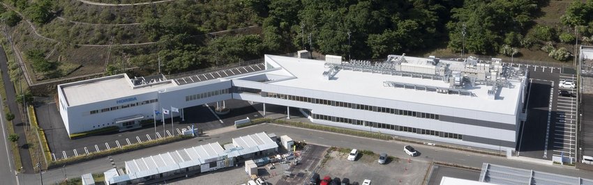
HORIBA STEC Co., Ltd. (President: Dan Horiba), which leads the HORIBA Group’s semiconductor business, announces that the newly added expandedfacilities at HORIBA’s R&D base, the Kyoto Fukuchiyama Technology Center, has begun full-scale operation.
The Kyoto Fukuchiyama Technology Center, established in 2013 as the Group’s first facility specializing in R&D activities for semiconductor industry, has obtained ISO/IEC 17025*1 accreditation for the calibration of gas mass flow rates*2. The facility’s efforts have improved the quality of mass flow controllers (MFCs), a core product. one of HORIBA STEC’s core products.
As a result of the facilities expansion, the processing capacities of both the gas flow calibration facilities and the liquid vaporization testing facilities have doubled. By enabling testing and calibration across a broader measurement range than before, this expansion bolsters strengthens the company’s ability to accommodate new materials required in state-of-the-art semiconductor processes. In addition, this expansion establishes a robust foundation for considering further production capacity enhancements from a medium- to long-term perspective.
In addition, the largest area of the newly constructed building has been designed as a new Engineering Room dedicated to advancing the use of cutting-edge technologies. Based on the findings of research conducted at this facility, the company will promote the development of highly precise digital twin*3 models that leverage the HORIBA Group’s advanced data management capabilities. These models will contribute to further enhancing the functionality of MFCs and accelerating development cycles.
In coordination with the Kyoto Fukuchiyama Factory, currently under construction on the adjacent site and scheduled to begin operation in spring 2026, the company will also pursue synergies that enable the rapid implementation of the cutting-edge technologies developed at this facility, with the aim of expanding and growing its semiconductor business.

[Details of the Expansion]
1. Strengthening the R&D framework through the expansion of existing functions
Doubling the processing capacity of the gas flow calibration facilities will enhance capabilities for testing and calibration in both micro-flow and high-flow ranges, with a view toward to expanding applications, not only for MFCs, but also into other business fields.
In addition, the processing capacity of the liquid vaporization test facilities will be roughly doubled in order to accommodate new liquid and solid materials used in state-of-the-art semiconductor manufacturing processes. Other experimental areas will also be expanded to boost the ability to accommodate diverse processes and applications.
2. Establishment of new laboratories to accelerate enhancement of existing products and development of new products
・Plasma Laboratory
The company will advance research into technologies for generating, measuring, and controlling plasma, with the aim of expanding into new fields, such as cleaning process chambers for semiconductor manufacturing equipment and developing low-damage processes. In addition, by combining these efforts with HORIBA’s various process monitoring technologies, the company will accelerate research and development of new plasma applications as well as the development of new products, positioning this as one of its key domains for the future.
・Engineering Room
The company will collect vast quantities of experimental and operational data obtained from high-speed, digitally enabled MFCs using HORIBA’s unique proprietary data management system in order to establish digital twin models capable of predicting flow rates, degrees of component degradation, and service lives in areas that have traditionally been difficult to measure.
Furthermore, by collaborating with group Groupcompanies, including HORIBA Instruments’ HORIBA Reno Technology Center in the United States and HORIBA MIRA Ltd. in the United Kingdom, which engages in vehicle development engineering and testing operations, the company will optimize its digital twin models and promote technology deployment across the entire HORIBA Group, thereby driving the creation of new value.
3. Promoting the creation of new businesses that contribute to reducing environmental impact
Semiconductor manufacturing processes make use of greenhouse gases, such as SF6 (sulfur hexafluoride). Accordingly, since similar gases are also handled in the research and development of MFCs, the company has been working to render these gases harmless through the use of abatement equipment. Moving forward, HORIBA will leverage its accumulated expertise in measuring and analyzing gases to independently develop equipment capable of more accurately evaluating the decomposition performance of abatement equipment. The company also aims to create new business opportunities. Through these efforts, the company will contribute to the realization of semiconductor manufacturing processes that place greater emphasis on reducing environmental impact.
Through this effort, the company aims both to create new business opportunities and to contribute to semiconductor manufacturing processes that place greater emphasis on reducing environmental impact.
4. Evolution into a hub for accelerated innovation
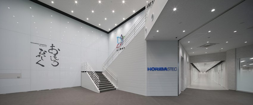
The design of the expanded facility incorporates elements that balance aesthetics with functionality, including open atriums and terraces with abundant natural light. The company has created a comfortable environment that makes work more pleasant and engaging, including a cafeteria that can also be used as a multipurpose space. In addition, new laboratory spaces dedicated to collaboration have been established to generate innovation through industry-academia-government coordination and inter-company partnerships. Furthermore, with the expansion of this facility and the launch of the Kyoto Fukuchiyama Factory, the site will function as a new, integrated hub, overseeing the entire process from R&D through to production, contributing to job creation in the region and the retention of human capital*4.
*1 An international standard that defines the technical competence and quality management systems required for testing and calibration conducted by laboratories and calibration bodies. Compliance with this standard ensures the accuracy and reliability of test and calibration results on an international level.
*2 The mass of a fluid that passes over a given surface in a unit of time
*3 Technology for analysis and optimization using virtual models that accurately replicate physical phenomena
*4 At HORIBA, employees are regarded as valuable assets and are referred to as “human capital”
[Facility Overview]
Name | HORIBA STEC Kyoto Fukuchiyama Technology Center |
Established | December 2013 |
Location | 11-1 Miwa, Miwa-cho, Fukuchiyama City, Kyoto |
Site area | 9,457 m² |
Total floor area | 5,642 m² (Two-story structure) (Approximately four times larger than before the expansion) |
Start of construction | March 2024 |
Total investment | Approximately 4 billion yen |
Number of employees | 35 (as of December 2025) |