Browse Products

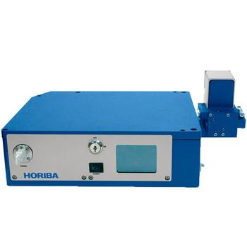
MicOS
Photoluminescence Microspectrometer

LabRAM Odyssey Semiconductor
Photoluminescence and Raman Wafer Imaging

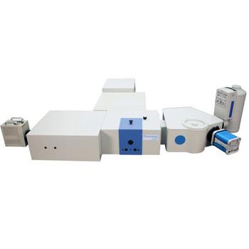
FluoroMax Plus
Steady State and Lifetime Benchtop Spectrofluorometer

Modular Raman Microscope
Flexible Raman System

LabRAM Soleil
Raman Spectroscope - Automated Imaging Microscope
Modular TeraHertz Raman Spectrometer
Affordable ultra-low frequency Raman spectrometer down to 10 cm-1

LabRAM HR Evolution
Confocal Raman Microscope
Nanolog
Steady State and Lifetime Nanotechnology EEM Spectrofluorometer
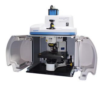
XploRA™ PLUS
MicroRaman Spectrometer - Confocal Raman Microscope

LabRAM Odyssey
Confocal Raman & High-Resolution Spectrometer

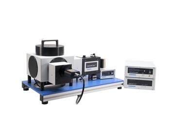
EasyLife L
Phosphorescence Lifetime Spectrometer
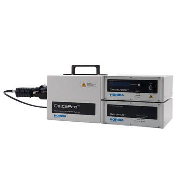
DeltaPro
TCSPC Lifetime Fluorometer

Duetta
Fluorescence and Absorbance Spectrometer
DeltaFlex
TCSPC/MCS Fluorescence Lifetime System

EasyLife X
Lifetime Fluorescence Spectrometer