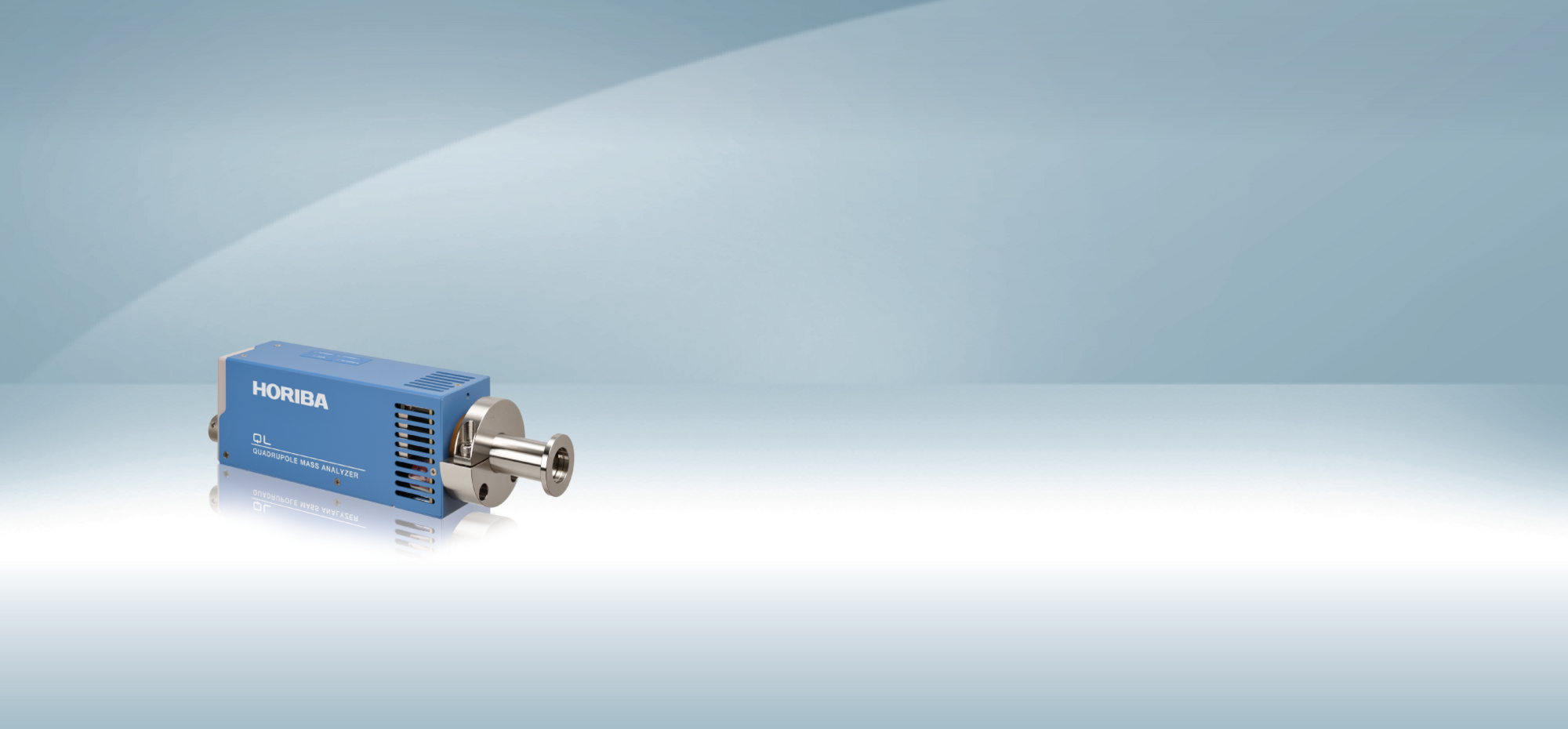
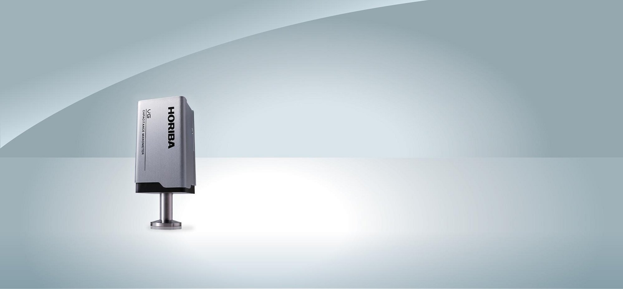
在当今社会,众多行业在拥挤的市场中寻求差异化,行业消费者的需求驱动着产品开发的换新速度。新技术以先进材料和半导体的应用为依托,而新技术的进步与运用又是新产品开发的核心。
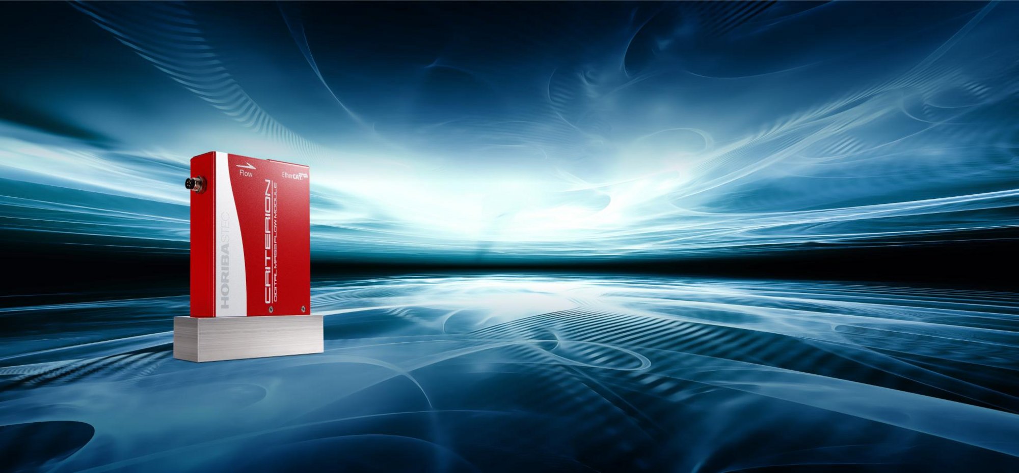
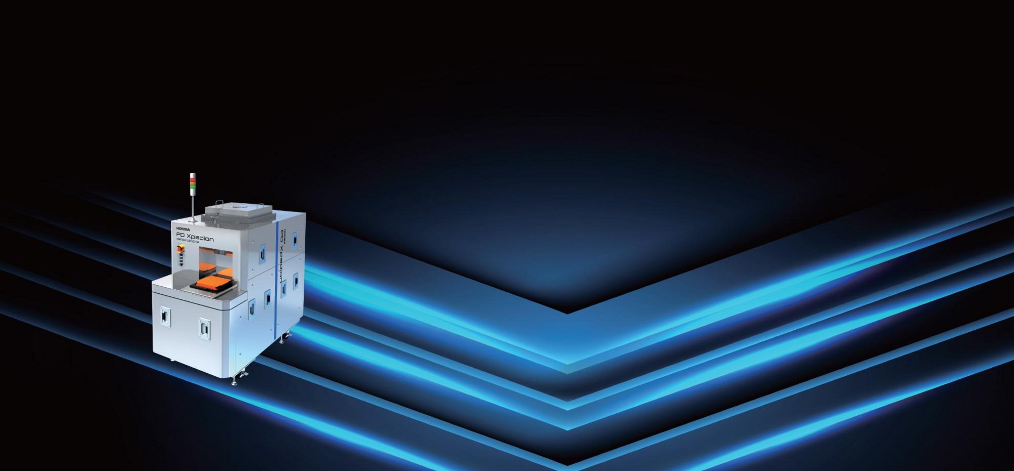
HORIBA 具备专业的流体控制、测量和分析能力,助力研发人员、设备制造商和最终用户提供符合全球需求的新颖解决方案
如您有任何疑问,请在此留下详细需求信息,我们将竭诚为您服务。
* 这些字段为必填项。