OmegaScope

OmegaScope, The AFM optical platform - Product image

The AFM optical platform

The OmegaScope is a state-of-the-art turn-key solution that combines Optics and ultra-resolution multi-range research AFM. The OmegaScope AFM is an advanced research instrument that provides path for researchers in spectroscopy and photonics. It is available in reflection configurations providing direct top and side optical access. The flexibility of the OmegaScope platform offer almost endless possibilities in correlation of high spatial resolution spectroscopies (Raman, Photoluminescence, Fluorescence) and AFM imaging modes.

Segment: Scientific
Manufacturing Company: HORIBA France SAS

No inteference of AFM registration laser with Raman excitation laser

1300 nm AFM laser does not interfere with the most popular UV, visible and near-IR Raman excitation lasers (364-830 nm) and eliminates any parasitic influence on VIS light-sensitive biological and photovoltaic samples.


Direct (below objective) pathway to cantilever

The OmegaScope system has the AFM and optical channels completely separated. Such independence does not limit the required wavelength of Raman laser and simplifies a lot the whole system adjustment in comparison with the systems where the AFM laser comes through the same high aperture objective as the Raman excitation laser. The user can easily re-focus the high aperture objective without any additional re-adjustment of the AFM laser-to-cantilever setup. The design of the OmegaScope also provides much more AFM stability and less sensitivity to any vibrations and acoustic noise.


Easy, quick and repeatable cantilever’s adjustment

The excitation laser to cantilever’s tip adjustment has never been so easy and quick before due to the fixed AFM laser design. Moreover, as soon as a new cantilever of the same type is installed, the same spot (within a few microns repeatability) on your sample surface can be easily found and scanned without any extra searching steps.


Automated AFM registration system adjustment

The SmartSPM scanning probe microscopes is the core of the reflection configuration of the OmegaScope system and at the same time is the first SPM with the automated/motorized laser-cantilever-photodiode alignment designed from the ground up for coupling with HORIBA spectrometers.


Fast scanning

Scanner resonant frequencies >7kHz in XY and >15kHz in Z are the highest in the AFM industry today.

Optimized scanner control algorithms make possible to scan much faster than ever before!


Vibration stability, Acoustic stability, Fast scanner with high resonant frequencies

Fast response time, low drift and metrological traceability. The best in the industry flexure based closed loop scanner with 100x100x15 micron scan range allows measurements of large areas and in the same time provides the true molecular resolution imaging. The high mechanical stiffness of the scanner and the whole AFM is the key to the outstanding OmegaScope performance without active vibration protection. These unique properties also allow the realization of special and more complicated scanning algorithms such as Top mode. In this mode the probe is lifted up above the sample surface between scanning points. In each scanning point the probe is approached back to the surface. The scanning signal is measured right after the tip oscillation amplitude reaches the set threshold. It makes possible to avoid any lateral force interactions and for example secure TERS probes, but at the same time keep the scanning rate up to 1 Hz.


Ease of sample replacement

The OmegaScope AFM platform design allows changing samples with the AFM head and cantilever holder in place. It seriously improves the reliability of experiments and protects the system from possible operator’s mistakes during such kind of routine procedures.


Top and side optical access

Top and Side optical access to the tip-sample area is provided to be able to explore the full capabilities of correlated AFM and spectroscopic imaging using IR, VIS and UV high NA planapochromat objectives (top objective: up to 0.7 NA; side objective: up to 0.7 NA), which enable confocal detection of optical signal from the sample surface in a wide spectral range and the minimum size of excitation laser spot area. The properly designed side optical channel of the OmegaScope system plays an extremely important role in successful TERS and TEPL experimentation as it provides a much more significant Z component of the optical field and effectively excites the Plasmon resonance in the tip-sample junction.


Top and side objective scanners

To perfectly align the AFM tip and Raman laser beam, the flexure-guided closed loop XYZ objective scanners can be installed in the top, side and bottom channels. Moreover, such solution provides the highest possible resolution, long-term stability and alignment automation, plus a wider spectral range with the less number of optical components in the light input/output system and consequently the less waste of useful optical signal.


Built-in DFM measuring made with PLL

The Dynamic Force Microscopy (DFM) mode comes as the standard option of the OmegaScope system. A frequency modulation (FM) detector for this mode is designed by utilizing the phase-locked loop (PLL) circuit built-in in the AIST-NT’s controller. Using DFM one can reliably maintain the minimal tip-sample interactions (i.e. operation in the field of attractive forces) which can appear very crucial for successful TERS and Scanning Near-field Optical Microscopy (SNOM) experiments.


STM, Conductive AFM and SNOM options

Simultaneously with spectroscopy measurements OmegaScope can be equipped with the unique module, using which one can measure local currents in AFM or STM in three linear ranges (1 nA, 100nA and 10 uA). These ranges can be switched within the software, where for each of them the required bandwidth can be selected from 100Hz to 7 kHz. The conductive module noise level of 60 fA in the measuring range up to 1 nA and 1300 nm AFM laser just sets the new standard for conductivity measurements in the field of photovoltaics.

In addition to the exceptional flexibility of the OmegaScope platform, the SNOM option based on the tuning fork feedback design can be easily included. Besides the standard SNOM experiments, you may follow the classics of nano-optics, especially apertureless SNOM, with a system for near-field fluorescence imaging using a metal tip illuminated with femtosecond laser pulses of proper polarization.


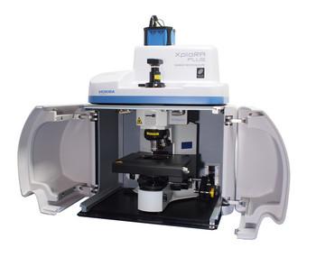
SmartSPM Scanner and Base

Sample scanning range: 100 µm x 100 µm x 15 µm (±10 %)

Scanning type by sample: XY non-linearity 0.05 %; Z non-linearity 0.05 %

Noise: 0.1 nm RMS in XY dimension in 200 Hz bandwidth with capacitance sensors on; 0.02 nm RMS in XY dimension in 100 Hz bandwidth with capacitance sensors off; < 0.04 nm RMS Z capacitance sensor in 1000 Hz bandwidth

Resonance frequency: XY: 7 kHz (unloaded); Z: 15 kHz (unloaded)

X, Y, Z movement: Digital closed loop control for X, Y, Z axes; Motorized Z approach range 18 mm

Sample size: Maximum 40 x 50 mm, 15 mm thickness

Sample positioning: Motorized sample positioning range 5 x 5 mm

Positioning resolution: 1 µm
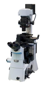
 

AFM Head HE002

Laser wavelength: 1300nm;

No registration laser influence on biological sample;

No registration laser influence on photovoltaic measurements;

Registration system noise: <0.1nm;

Fully motorized: 4 stepper motors for cantilever and photodiode automated alignment;

Free access to the probe for additional external manipulators and probes;

Top and side simultaneous optical access: with planapochromat objectives, Side objective up to 100x, NA=0.7 Top objective 10x, NA=0.28 simultaneously;
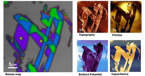
 

SPM Measuring Modes

Contact AFM in air/(liquid optional); Semicontact AFM in air/(liquid optional); Non -contact AFM; Phase imaging; Lateral Force Microscopy (LFM); Force Modulation; Conductive AFM (optional); Magnetic Force Microscopy (MFM); Kelvin Probe (Surface Potential Microscopy, SKM, KPFM); Capacitance and Electric Force Microscopy (EFM); Force curve measurement; Piezo Response Force Microscopy (PFM); Nanolithography; Nanomanipulation; STM (optional); Photocurrent Mapping (optional); Volt-ampere characteristic measurements (optional).


Measuring SPM Modes simultaneously with Raman measurements

Contact AFM in air;

Contact AFM in liquid (optional);

Semicontact AFM in air;

Semicontact AFM in liquid (optional);

Dynamic Force Microscopy (DFM, FM-AFM);

Dissipation Force Microscopy;

True Non-contact AFM;

Phase Imaging;

Lateral Force Microscopy (LFM);

Force Modulation;

Conductive AFM (optional);

Single-pass Kelvin Probe;

Piezo Response Force Microscopy (PFM);

STM (optional);

Photocurrent Mapping (optional);

Shear-force Microscopy with tuning fork (ShFM) (optional);

Normal Force Microscopy with tuning fork (optional).


Spectroscopy Modes

Confocal Raman, Fluorescence and Photoluminescence imaging and spectroscopy

Tip-Enhanced Raman Spectroscopy (TERS) in AFM, STM, and shear force modes

Tip-EnhancedPhotoluminescence (TEPL)

Near-field Optical Scanning Microscopy and Spectroscopy (NSOM/SNOM).


Conductive AFM Unit (optional)

Current range:  100 fA ÷ 10 µA; 3 current ranges (1 nA, 100 nA and 10 µA) switchable from the software.


Optical Access

Capability to use simultaneously top and side plan apochromat objective: Up to 100x, NA = 0.7 from top or side; Up to 20x and 100x simultaneously.

Closed loop piezo objective scanner for ultra stable long term spectroscopic laser alignment: Range 20 µm x 20 µm x 15 µm; Resolution: 1 nm   

TERS Characterization of Lipid Nanotubes as Carbonaceous Material for Electrodes
For thirty years there has been a research focused onto carbonization of 3D structures especially to be employed in electronic applications. These structures are prepared with the help of lithography and pyrolyzed afterwards. For making features below 100 nm, a bottom-up approach using lipids nanotubes is attempted.
TERS Characterization of Single- to Few-Layer Ti₃C₂Tₓ MXene
MXenes is the largest and fastest growing 2D materials. They have unique properties such as good conductivity and a hydrophilic surface. The control of nanoscale composition would ultimately allow for engineering properties locally, gaining more control over the 2D material-based systems.
TERS on Functionalized Gold Nanostructures for Nano-scale Biosensing
Surface-enhanced Raman scattering (SERS) is a powerful plasmonics-based analytical technique for biosensing. SERS effect relies on nanostructures that need to be designed to maximize enhancement factors and molecular specificity. In addition to numerical modeling, an analytical tool capable of imaging localized enhancement would be an added value.
TERS Characterization of phospholipid bilayers and detection of nanoparticles
Phospholipid bilayers, major constituents of membranes act as a barrier of selective permeability for the nanoparticles now largely into our environment. Studying the interactions between nanoparticles and cellular membranes requires a molecular chemical probe with nanometer resolution capability.
TERS Characterization of Graphene Nanoribbons
Graphene is foreseen for a handful of electronic and optoelectronic nano-devices. Making nano-devices out of graphene requires nanopatterning. Determining the quality of patterned graphene is essential and the detection of defects demands a sensitive chemical nano-characterization tool.
TERS Characterization of Explosive Nanoparticles
It is not yet understood how co-crystal nanoparticles (co-crystallinity combined with nanostructuring) have superior properties to single compound crystals. Only a technique capable of probing single nanoparticles can bring answers.
c-AFM and in operando TERS & µRaman Characterization of Molecular Switching in Organic Memristors
Emergence of organic memristors has been hindered by poor reproducibility, endurance stability scalability and low switching speed. Knowing the primary driving mechanism at the molecular scale will be the key to improve the robustness and reliability of such organic based devices.
Correlated TERS and KPFM of Graphene Oxide Flakes
Visualizing the distribution of structural defects and functional groups present on the surface of two-dimensional (2D) materials such as graphene oxide challenges the sensitivity and spatial resolution of most advanced analytical techniques.
AFM-TERS measurements in a liquid environment with side illumination/collection
Atomic Force Microscopy (AFM) associated to Raman spectroscopy has proven to be a powerful technique for probing chemical properties at the nanoscale. TERS in liquids will bring promising results in in-situ investigation of biological samples, catalysis and electrochemical reactions.
Characterization of Nanoparticles from Combustion Engine Emission using AFM-TERS
A new concern for human health is now raised by sub-23 nm particles emitted by on-road motor vehicles. Beyond measuring particle number and mass, it is also critical to determine the surface chemical composition of the nanoparticles to understand the potential reactivity with the environment.
Correlated TERS, TEPL and SPM Measurements of 2D Materials
Many challenges remain before the promise of 2D materials is realized in the form of practical nano-devices. An information-rich, nanoscale characterization technique is required to qualify these materials and assist in the deployment of 2D material-based applications.
Characterization of MoS2 Flakes using TEOS
Both TEPL and TERS images are well correlated with AFM morphological images obtained simultaneously, and all are consistent in revealing the nature (number of layers) of MoS2 flakes. Upon deconvolution, the TEPL signal is even capable of revealing local inhomogeneities within a MoS2 flake of 100 nm size. Kelvin probe measurement supports TEPL and TERS measurements and adds to the power of such tip-enhanced combinative tools. TEOS characterization of 2D materials is likely to contribute to further deployment of these materials into commercial products through a better understanding of their electrical and chemical properties at the nanoscale.
Characterization of Carbon Nanotubes Using Tip-Enhanced Raman Spectroscopy (TERS)
The use of TERS to reveal the defects density in the structure of CNTs is of interest for a better understanding of the electrical properties of the devices made with such nano-objects. Not only defects concentration but also local chirality changes from the different radial breathing modes, pressure effect and strain distribution can be studied at the single carbon nanotube level through TERS.
Characterization of Graphene using TERS

Request for Information

Do you have any questions or requests? Use this form to contact our specialists.

* These fields are mandatory.

Related products

LabRAM Odyssey
LabRAM Odyssey

Confocal Raman Imaging & High Resolution Spectrometer

LabRAM Odyssey Nano
LabRAM Odyssey Nano

AFM-Raman for physical and chemical imaging

LabRAM Soleil
LabRAM Soleil

Multimodal Confocal Raman Microscope

LabRAM Soleil Nano
LabRAM Soleil Nano

Real-time and Direct Correlative Nanoscopy

TRIOS
TRIOS

Versatile AFM Optical Coupling

XploRA Nano
XploRA Nano

AFM-Raman for Physical and Chemical imaging

XploRA™ PLUS
XploRA™ PLUS

Raman Spectrometer - Confocal Raman Microscope

CombiScope
CombiScope

AFM and inverted light microscopy

CS-100 Series
CS-100 Series

Stand-alone Type Chemical Concentration Monitor

CS-100F1 Series
CS-100F1 Series

Fiber Optic Type Chemical Solution Concentration Monitor

CS-700
CS-700

High Precision, High Stability Chemical Concentration Monitor

TRIOS
TRIOS

Versatile AFM Optical Coupling

CombiScope
CombiScope

AFM and inverted light microscopy

SmartSPM
SmartSPM

Advanced stand-alone AFM

TRIOS
TRIOS

Versatile AFM Optical Coupling

Corporate