
HORIBA, Ltd. has selected the winners of the 2023 Masao Horiba Awards for promotion of research in analytical and measurement technologies from among scientists and engineers at universities and public research institutes worldwide. Established in 2003, the 19th Masao Horiba Awards this year received 33 entries from scientists and engineers worldwide for their work Analysis and measurement technologies that contribute to the realization of cutting-edge semiconductor devices. The screening committee composed of seven judges including prestigious scientists and engineers in the field selected three winners and two honorable mention after evaluating each entry with focus on the promise, originality, and potential as a unique measurement instrument.
We are honored to hold the award ceremony inviting not only the winners but also academics and government officials to the award ceremony and commemorative seminar held at the Kyoto University on Oct 17.
Award Winners and Their Award-Winning Research
【Masao Horiba Awards】
Dr. Ryota Ishii
Assistant Professor
Department of Electronic Science and Engineering, Kyoto University
“Exploring spatially and temporally resolved deep-ultraviolet spectroscopy toward understanding and controlling optoelectronic properties of ultrawide bandgap semiconductors”
Dr. Naresh Kumar
Senior Scientist
Department of Chemistry and Applied Biosciences, ETH Zurich
“Nanoscale Chemical Characterization of Novel Semiconductor Materials using Tip-Enhanced Optical Spectroscopy”
Dr. Ang-Yu Lu
PhD Student
Department of Electrical Engineering and Computer Science, Massachusetts Institute of Technology
“Unraveling the Correlation between Raman and Photoluminescence in Monolayer MoS2 through Machine-Learning Models”
【Masao Horiba Awards -Honorable Mention-】
Dr. Mitsuru Takenaka
Professor
School of Engineering, Department of Electrical Engineering and Information Systems, The University of Tokyo
“Electro-photonic Integrated Deep Learning Processor using Si Photonic Integrated Circuits”
Dr. Maki Kushimoto
Associate Professor/ Lecturer
Graduate School of Engineering, Nagoya University
“Development of a compact deep-ultraviolet laser source for precision microstructure measurement”
About Masao Horiba Awards
HORIBA, Ltd. established the Masao Horiba Awards in 2003 to commemorate its 50th anniversary. This award aims to support up-and-coming scientists and engineers both in Japan and overseas who are involved in research and development expected to bring about innovative analytical and measurement technologies, while helping further elevate the standing of measurement technologies in the science and technology field. The Masao Horiba Awards spotlight unique research and development of which results and future potential have global appeal by selecting specific themes within the analytical and measurement technologies field each year centered upon the principles and elemental technologies cultivated by the HORIBA Group.
Screening Committee for the 2023 Masao Horiba Awards
(Honorific titles omitted, in no particular order)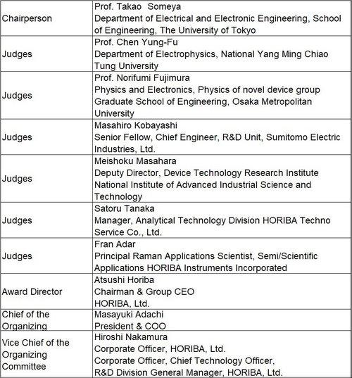
About the Award Ceremony
Date : Tuesday, October 17, 2023
Venue : Kyoto University
2023 Masao Horiba Awards Ceremony Program (Tentative)
1st Session: Commemorative Seminar (Starting at 2:30 p.m.)
・Winner presentations : Three winners and two honorable mention
2nd Session: Award Ceremony (Starting at 4:30 p.m.)
・Introduction of award-winning research
・Presentation of a certificate and prize money
・Greeting from Award Director Atsushi Horiba (Chairman & Group CEO, HORIBA, Ltd.)
Eligible Fields and Background of the 2023 Masao Horiba Awards
The recent wave of digitalization is transforming not only IT companies, but also all industries and socioeconomic systems, including manufacturing, mobility, services, agriculture, and healthcare.
Due to the expansion of digitalization, the amount of data processing continues to increase steadily, and it is becoming increasingly urgent that semiconductor devices used in Information and Communication Technologies related equipment be upgraded to higher performance. In response to these requirements, there are high expectations for further miniaturization, upscaling of new advanced materials to large substrates and manufacturing new complex 3D structures, leading to the development of innovative devices that didn’t exist before. On the other hand, compound semiconductors possess superior characteristics to that of silicon semiconductors in terms of their much faster electron transfer speed, their capabilities of high-speed signal processing and low-voltage operation, and their abilities to respond to light and generate microwaves. As a result, compound semiconductors have grown to be widely used in our daily lives as key materials in semiconductor devices that support digitization. Power semiconductors are used to control a wide variety of electrical devices in our daily lives, including automobiles, industrial equipment, electric power grids, railroads, and home appliances. To realize carbon neutrality, more technological innovations for saving energy are expected. On the other hand, the establishment of innovative electrical transmission technology is also important to achieve higher device speeds and power savings. From this perspective, the establishment of optoelectronics technology that integrates light and electronics for information and communication processing is urgently needed, and the development of optoelectronic devices and optoelectronic fusion processors for the Beyond 5G/6G all-optical era is paramount. In addition, further understanding of phenomena such as superconductivity, ion trapping, and light is needed to realize quantum computers, which will require new analytical and measurement techniques for characterization of devices and products.
Semiconductor devices are built using a wide variety of technologies, from raw materials to wafer fabrication, manufacturing processes, and integration schemes. Analytical and measurement technologies are indispensable in all processes, from the fundamental research level to prototyping and production optimization. Especially in the practical application of innovative devices such as power devices, optical devices, and quantum devices, it is important to find scientific explanation of previously unencountered phenomena and identify control points in prototyping and manufacturing, for which analytical and measurement technologies are becoming increasingly important.
The 2023 Masao Horiba Award is open to advanced analytical and measurement technologies necessary to solve these problems and consequently provide next-generation devices to the world. We have decided to shine a light on the researchers and engineers who are working on the development of such analytical and measurement technologies and whose results will lead to advancement in use cases and applications for next-generation devices, such as system autonomy, innovations in transportation, and wearable devices for health and medicine.
Winners and their award-winning research
【Masao Horiba Awards】
Dr. Ryota Ishii
Assistant Professor
Department of Electronic Science and Engineering, Kyoto University
“Exploring spatially and temporally resolved deep-ultraviolet spectroscopy toward understanding and controlling optoelectronic properties of ultrawide bandgap semiconductors ”
Ultrawide bandgap* (UWBG) semiconductors have attracted much attention as next-generation semiconducting materials because of their extremely large bandgap. Diamond, gallium oxide (Ga2O3), and aluminum nitride (AlN) are typical examples of UWBG semiconductors, and it is expected that efficient deep-ultraviolet light-emitting devices* and ultra-low-loss/high-voltage power devices will be realized using UWBG semiconductors.
However, the luminous efficiency* of deep-ultraviolet light-emitting diodes based on UWBG semiconductors is currently very low. Dr. Ishii attributed it to the incomplete understanding of UWBG semiconductor physics, and further focused on the immaturity of deep-ultraviolet spectroscopy* which is one of the analysis and measurement techniques for UWBG semiconductors. Dr. Ishii has been investigating the optoelectronic properties of UWBG semiconductors by exploring spatially and temporally resolved deep-ultraviolet spectroscopy. These include the development of a deep-ultraviolet spectroscopic system under perturbation* uniaxial stress/electric) field and a deep-ultraviolet scanning near-field optical microscope* operating at the world’s shortest wavelength, the elucidation of the exciton fine structure* of AlN, and the observation of a radiative recombination defect in aluminum-gallium-nitride (AlGaN) quantum well structures. These studies should accelerate the development of UWBG semiconductor devices and technologies.
* Wide Bandgap:
Refers to semiconductors with a large bandgap. The bandgap is a barrier within the semiconductor that electrons cannot pass through, and the wider the bandgap, the more restricted the movement of electrons. It is a crucial factor determining the electrical and optical properties of the semiconductor.
* Deep-ultraviolet light-emitting device:
A device that emits light in the deep ultraviolet region. The deep ultraviolet region has a very short wavelength and higher energy compared to typical light.
* Luminous efficiency:
A measure of how much light output a device can achieve relative to the input power supplied to it.
* Deep ultraviolet spectroscopy:
A technique used to analyze the properties of materials using light in the deep ultraviolet region. By measuring how materials react to deep ultraviolet light, their characteristics and structures can be understood.
* Perturbation:
The change in external forces or electric fields applied to a system. Under perturbation, the properties and behavior of materials may change.
* Near-field optical microscope:
A high-resolution microscopy technique that allows the observation of small structures using light at optical wavelengths but using near field techniques to improve the spatial resolution.
* Exciton fine structure:
The state in which electrons and holes are bound together in a semiconductor material. Excitons are generated by absorbing energy such as light or an electric field, and they possess specific energy states.
Dr. Naresh Kumar
Senior Scientist
Department of Chemistry and Applied Biosciences, ETH Zurich
“Nanoscale Chemical Characterization of Novel Semiconductor Materials using Tip-Enhanced Optical Spectroscopy”
Dr. Kumar’s research focuses on the nanoscale investigation of two classes of semiconductor materials: two-dimensional (2D) transition metal dichalcogenides (TMDs) and organic photovoltaic (OPV) devices. In the study of 2D TMDs, Dr. Kumar utilized tip-enhanced optical spectroscopy (TEOS) to investigate excitonic processes in single-layer (1L) MoS2 and WSe2. Through hyperspectral tip enhanced photoluminescence imaging, he demonstrated an unprecedented spatial resolution of 20 nm in mapping exciton and trion populations in 1L MoS2. In the case of 1L WSe2, Dr. Kumar combined TEOS with Kelvin probe force microscopy to reveal the optoelectronic behavior of grain boundaries (GBs) at a resolution of 50 nm. For OPV devices, Dr. Kumar introduced a novel methodology called simultaneous topographical, electrical, and optical microscopy (STEOM) by combining TEOS with photoconductive-AFM (PC-AFM). This innovative approach enabled the simultaneous characterization of topography, chemical composition, and photoelectrical properties of an operational OPV device with sub-20 nm resolution.
The significance of Dr. Kumar’s research lies in the advancements made in nanoscale characterization and understanding of novel semiconductor materials. He has expanded the capabilities of TEOS by applying it to 2D TMDs and OPV devices, surpassing the limitations of conventional techniques. His findings provide valuable insights into excitonic processes, heterogeneity of exciton and trion populations, optoelectronic behavior of GBs, and the structure property relationships in OPV devices. Dr. Kumar’s research on the development of novel nanoanalytical technologies is expected to contribute significantly to the development and optimization of next-generation optoelectronic devices and organic photovoltaic technologies.
Dr. Ang-Yu Lu
PhD Student
Department of Electrical Engineering and Computer Science, Massachusetts Institute of Technology
“Unraveling the Correlation between Raman and Photoluminescence in Monolayer MoS2 through Machine-Learning Models”
Two-dimensional (2D) transition metal dichalcogenides (TMDCs)* with intense and tunable photoluminescence (PL)* have opened up new opportunities for optoelectronic and photonic applications such as light-emitting diodes, photodetectors, and single-photon emitters. Among the standard characterization tools for 2D materials, Raman spectroscopy stands out as a fast and non-destructive technique capable of probing material crystallinities and perturbations, such as doping and strain. However, due to its highly nonlinear nature, a comprehensive understanding of the correlation between PL and Raman spectra in monolayer MoS2 remains elusive.
In this work, Dr. Lu has systematically explored the connections between PL signatures and Raman* modes, providing comprehensive insights into the physical mechanisms correlating PL and Raman features. This analysis further disentangles the strain and doping contributions from the Raman spectra through machine-learning models. First, he deployed a DenseNet* to predict PL maps using spatial Raman maps*. Moreover, he applyed a gradient-boosted trees model (XGBoost)* with Shapley additive explanation (SHAP)* to evaluate the impact of individual Raman features on PL features, allowing him to link the strain and doping of monolayer MoS2. Lastly, Dr. Lu adopted a support vector machine (SVM)* to project PL features onto Raman frequencies. This work may serve as a methodology for applying machine learning in 2D material characterizations and providing the knowledge for tuning and synthesizing 2D semiconductors for high-yield PL.
* Two-dimensional transition metal dichalcogenides (TMDC):
Compounds consisting of transition metal elements and chalcogen elements such as sulfur, selenium, and tellurium, which have a two-dimensional layered structure.
*Photoluminescence (PL):
A phenomenon in which electrons in a material absorb light and emit light specific to that material.
*Raman emission:
A phenomenon in which the crystal lattice of a material scatters light specific to that material. The scattered light can be spectrally analyzed to determine the characteristics of the material.
*DenseNet:
A convolutional neural network used to learn features of images and patterns. Convolution refers to the process of detecting local patterns within an image.
*Spatial Raman map:
A mapping of Raman spectra obtained from different positions on the surface of a material using Raman spectroscopy.
*XGBoost (gradient-boosted trees model):
A machine learning algorithm known as gradient boosting.
*SHAP (Shapley additive explanation):
A method for evaluating the contribution of features to the predictions of a machine learning model.
*SVM (Support Vector Machine):
A machine learning algorithm used for tasks such as classification and regression.
【Masao Horiba Awards -Honorable Mention-】
Dr. Mitsuru Takenaka
Professor
School of Engineering, Department of Electrical Engineering and Information Systems, The University of Tokyo
“Electro-photonic Integrated Deep Learning Processor using Si Photonic Integrated Circuits”
Prof. Takenaka has conducted pioneering research on the application of devices that integrate heterogeneous materials such as compound semiconductors, phase-change materials, and two-dimensional materials into silicon photonic devices for deep learning processors.
Deep learning processors utilizing reconfigurable silicon photonic circuits (programmable photonic circuits) are expected to be capable of performing high-speed, low-power, and low-latency summation and multiplication operations, thereby improving the performance of artificial intelligence (AI) regardless of semiconductor miniaturization. Research on this next-generation computing technology is being conducted worldwide. However, in practical-scale programmable photonic circuits, precise measurement and control of optical phase within the circuit and measurement techniques that can convert optical operation results into low-power and high-speed photodetection are of utmost importance.
Prof. Takenaka has been challenging the precise measurement and control of optical phase and intensity within photonic circuits by integrating compound semiconductors and phase-change materials into silicon photonic circuits. He is also engaged in research to achieve a new programmable photonic circuit that allows learning acceleration through error backpropagation on the optical circuit. These achievements are expected to greatly contribute to the early realization of deep learning processors using silicon photonic circuits.
*Compound semiconductor:
A semiconductor material composed of multiple elements, exhibiting a wide range of physical and electronic characteristics and offering advantages such as high electron mobility and improved optical properties.
*Phase-change materials:
Materials that exhibit the property of changing their phase (state) in response to variations in temperature or pressure.
*Two-dimensional materials:
Materials that are extremely thin, with a surface structured in a two-dimensional manner. They are composed of atomic or molecular monolayers or a few layers.
*Photonic-Deep Learning Processor:
An integrated circuit designed to perform specialized digital information processing by combining photonic and electronic circuits. It is used to execute the machine learning technique called deep learning.
*Reconfigurable silicon photonic circuit (programmable photonic circuit):
A silicon-based circuit that can control the flow of light through programming.
*Optical phase:
Information related to the position and direction of propagation of light waves.
*Measurement technique that converts optical computational results into optoelectronic signals:
A technique that converts computational results performed within an optical circuit into electrical signals and reads the data.
*Error backpropagation:
A learning method in neural networks where errors are propagated in the reverse direction to adjust the weights and biases, enabling accurate output generation.
Dr. Maki Kushimoto
Associate Professor/ Lecturer
Graduate School of Engineering, Nagoya University
“Development of a compact deep-ultraviolet laser source for precision microstructure measurement”
In this study, Dr. Kushimoto has demonstrated a compact deep ultraviolet semiconductor laser that can be integrated into high-resolution and high-precision measurement systems, supporting technological innovations in the semiconductor industry where miniaturization is advancing. Furthermore, she has successfully achieved room temperature continuous wave lasing.
Laser light is used in non-contact and non-destructive optical analysis and measurement techniques. Laser light with shorter wavelengths can detect finer structures, making short-wavelength laser light sources increasingly important. Semiconductor lasers have been widely used as compact, high-efficiency, and low-cost light sources in inspection systems. However, there have been many challenges in realizing semiconductor lasers that emit deep ultraviolet light.
Therefore, Dr. Kushimoto succeeded in realizing a deep ultraviolet semiconductor laser through the reduction of defect density in AlGaN using single-crystal AlN substrates and the use of a conductivity control technique different from conventional methods, involving pulse current injection. Furthermore, she constructed a measurement system for comprehensive evaluation and revealed that the deterioration of device performance is primarily caused by defect formation. Dr. Kushimoto proposed a method to suppress the concentration of shear stress through shape control of the laser crystal. As a result, she achieved a room temperature continuous wave lasing that operates at one-tenth of the initial power. This achievement greatly contributes to the practical application of deep ultraviolet semiconductor laser light sources.
The affiliation, position, etc. of the winners are as of the time of application.
