<< Back to OEM Solutions for Semiconductors
In the semiconductor industry, the fabrication of devices such as 3D memory chips, logic electronics, MEMS sensors, lighting components (LED, OLED, QCL, Laser diodes…) and flat panels relies on plasma processes, such as dry etch, cleaning and plasma CVD.
With the advent of 3D technology, faster and deeper etching is necessary to produce multi-stacked thin films (sometimes with several hundred layers) with nanometer-sized features. In turn, this increases the need for fast and precise control of plasma deposition and etching steps to ensure the performance and reliability of the manufacturing process.
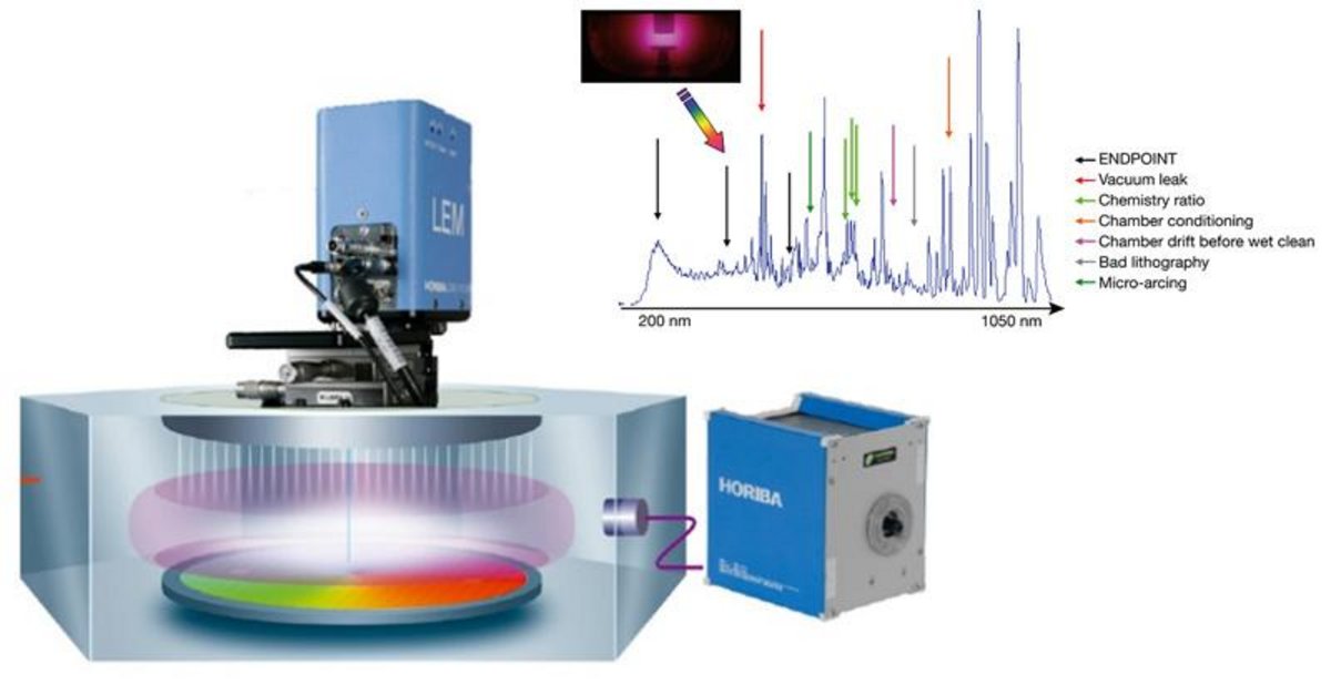
Optical Emission Spectroscopy (OES) and (Multiwavelength) Interferometry play a crucial role in the process control of semiconductor manufacturing, offering a powerful means to remotely monitor the plasma and control thickness and interface evolution on wafer in real time to detect the process endpoint.
HORIBA has introduced a unique generation of sensors dedicated to advanced endpoint control, fault detection and chamber health monitoring.
Plasma monitoring | Endpoint detection | Etch and deposition control | Chamber cleaning | Tomographic OES | HORIBA solutions
OES is used to monitor plasma by analyzing emitted light. Spectrometers detect optical emission of light with spectral peaks corresponding to different elements and compounds present in the plasma. By doing so, OES can provide real-time data on the plasma's composition and behavior, such as the presence and concentration of specific ions and radicals.
This is essential for maintaining the stability and repeatability of the plasma conditions, which directly affect the wafer quality and production yields.
The advantage of using high spectral resolution, high sensitivity and high-speed OES for plasma monitoring/deep etching lies in its ability to offer non-invasive, real-time analysis, ensuring optimal process control, transition detection and elimination of defects.
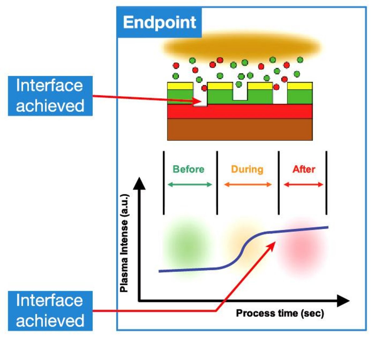
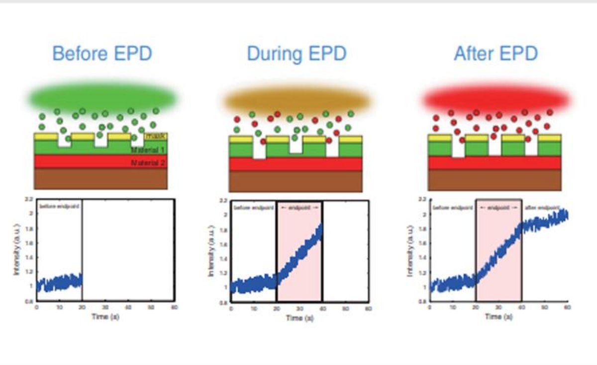
Determining the exact endpoint of processes like etching is critical in semiconductor fabrication, as it ensures that the material is removed or modified to the correct depth without over-etching or under-processing.
OES and (Multiwavelength) Interferometry are employed in endpoint detection by monitoring the changes in the emission spectra of the materials being processed. Spectrometers identify changes in the intensity of specific emission lines, indicating the completion of the etching process. This precise control ensures that the desired patterns are accurately processed onto the semiconductor wafers, improving yield and reducing waste.
This is essential for achieving high precision and repeatability, crucial for the complex and delicate structures of modern semiconductors.
The advantage of OES and (multiwavelength) Interferometry in endpoint detection are their sensitivity and accuracy, enabling tight control over process completion and enhancing product quality.
Etching and deposition are fundamental processes in semiconductor manufacturing that define the features and layers of devices.
Spectrometers analyze plasma by identifying specific wavelengths, which helps to accurately adjust the etch rate and uniformity. Real-time feedback enables adjusting gas flow rates and power levels, guaranteeing precise pattern transfer onto semiconductor wafers.
During deposition processes such as Chemical Vapor Deposition (CVD) and Physical Vapor Deposition (PVD), OES is employed to analyze emissions from process gases and the growing films. Spectrometers monitor the composition and thickness of the deposited layers, providing continuous feedback to optimize film quality. This ensures that the layers meet the required specifications for device performance.
This control is essential for the precision required in advanced semiconductor devices.
The primary advantage of OES in etch and deposition control is its ability to provide immediate feedback, leading to better process stability and reduced waste.
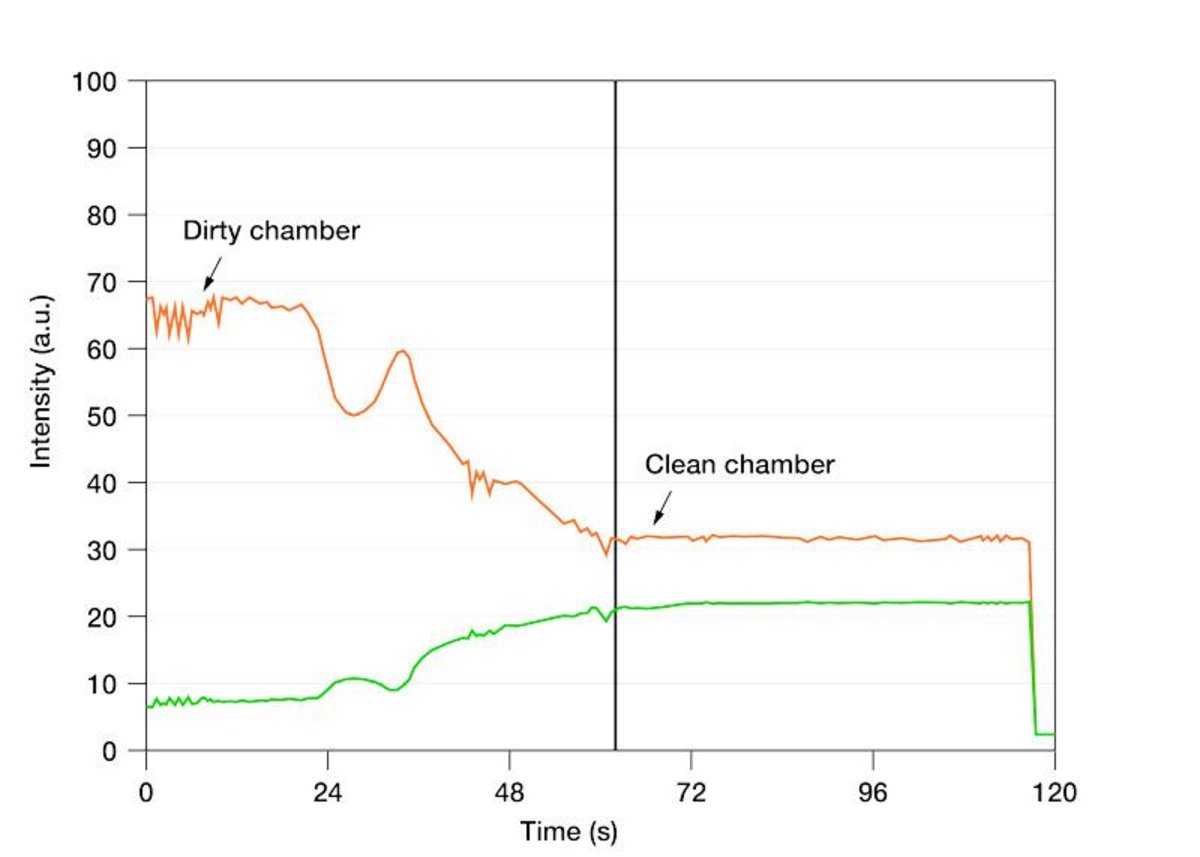
clean processing environment is critical in semiconductor manufacturing to prevent contamination and defects. Chamber cleaning requires a high-performance OES with ultra-high sensitivity.
Spectrometers are used to monitor the cleaning process of reaction chambers by detecting residual materials and by-products from previous processes. By analyzing the emission spectra during the cleaning cycle, OES can confirm when the chamber is free of contaminants, ensuring that the environment is properly prepared for the next batch of wafers.
This is essential for maintaining high yields and consistent product quality.
The advantage of using OES for chamber cleaning is its efficiency and effectiveness in verifying cleanliness without manual inspection, saving time and reducing the risk of contamination.
Tomographic Optical Emission Spectroscopy (TOES) enhances the capabilities of traditional OES by providing spatially resolved data on the distribution of plasma and materials within the processing chamber.
This advanced technique uses multiple lines of sight to create a detailed map of the plasma characteristics and material distribution. TOES is essential for understanding the complex dynamics within the chamber, allowing for more precise control of the process environment. However, with tools getting larger and structures getting smaller, uniformity becomes very challenging.
By analyzing the spatial distribution of emissions, TOES helps identify non-uniformities and optimizes the process conditions.
It requires OES with imaging spectrometer performance that have multitrack/multifiber spectrometers connecting to various windows/locations on the tools.
A hyperspectral version may also be used, with direct line imaging of a plasma segment onto the input slit of the OES.
The advantage of TOES is its ability to provide a comprehensive view of the process, leading to improved uniformity, accuracy and consistency in semiconductor fabrication.
HORIBA’s spectrometers provide high-performance optical analysis for semiconductor research. They enable precise plasma monitoring, hyperspectral imaging, and UV-VIS-NIR spectral measurements, ensuring accurate characterization of thin films, contamination detection, and process control in fabrication, optimizing semiconductor performance and yield in advanced manufacturing and R&D.

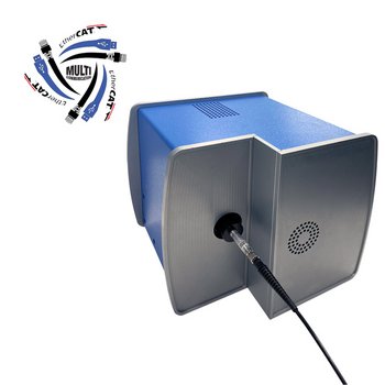
Endpoint / Chamber Health Monitor based on Optical Emission Spectroscopy and MWL Interferometry
UV-VIS-NIR Spectrometer
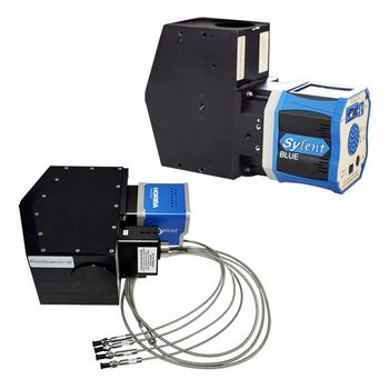
Multichannel Spectrometer and Hyperspectral Line Imager
Multispectra, Multifiber, Multichannel Imaging spectrometer with 8-16-32 Simultaneous UV-NIR Spectra

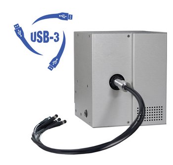
Miniature Multi Communication UV-NIR Spectrometer

High Spectral Rate and High Dynamic Range Miniature Spectrometers
Do you have any questions or requests? Use this form to contact our specialists.