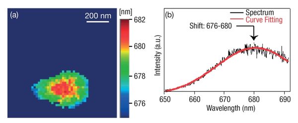


(a) TEPL-shift image and (b) Curve Fitting of PL signal
Molybdenum disulfide (MoS2) is a promising semiconducting Transition Metal Dichalcogenide (TMD) 2D nano-material for next generation photovoltaic solar cells, optoelectronic circuits and sensors due to its great excitonic recombination property, high carrier mobility and low leakage current.
One of the advantages of two dimensional (2D) TMDs, when compared to graphene, comes from quantum confinement, enabling the indirect-to-direct bandgap transition as a function of number of individual layers. Nano-scale characterization is needed for the understanding necessary to engineer nanodevices integrating monolayer MoS2.
Tip-enhanced optical spectroscopies (TEOS) based on the amplification of signal from the nano-region under the tip enables such nano-characterization. In the case of 2D TMD, Tip-Enhanced Photoluminescence (TEPL) is capable of revealing variation in emission within a submicron size flake. Complementary morphological, chemical, and electronic structure information may be acquired simultaneously and with nanometer spatial resolution through AFM imaging, Tip Enhanced Raman spectroscopy (TERS) and Kelvin probe measurements, respectively.
Real-time and Direct Correlative Nanoscopy
AFM-Raman for physical and chemical imaging
Raman Spectroscope - Automated Imaging Microscope
AFM-Raman for Physical and Chemical imaging
Versatile AFM Optical Coupling
Confocal Raman Microscope
MicroRaman Spectrometer - Confocal Raman Microscope
Confocal Raman & High-Resolution Spectrometer
The AFM optical platform
Sie haben Fragen oder Wünsche? Nutzen Sie dieses Formular, um mit unseren Spezialisten in Kontakt zu treten.