
From blank wafer to final device, HORIBA’s analytical instrument for material characterization are used by leading end-user and research organization for more than 50 years. Designed to achieve ultimate performances, they are the right tools to accelerate the time to market and yield improvement in any processes involving thin film and advanced material deposition.
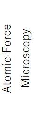 | 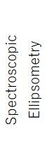 | 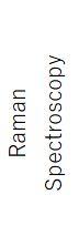 | 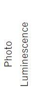 | 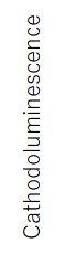 | 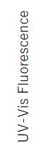 | 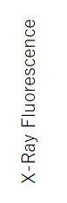 | 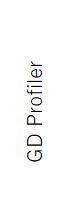 | 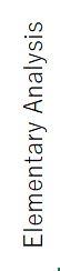 | 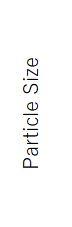 | |
Roughness | ● | ● | ● | |||||||
Film thickness | ● | |||||||||
Optical properties (n, k) | ● | |||||||||
Band Gap | ● | ● | ● | |||||||
Crystallinity | ● | ● | ||||||||
Stochiometry | ● | ● | ● | |||||||
Chemical composition | ● | |||||||||
Elemental composition | ● | ● | ● | |||||||
Defects | ● | ● | ● | |||||||
Impurities | ● | |||||||||
Stress measurement | ● | |||||||||
Doping concentration | ● | |||||||||
Particle sizing | ● |
Máte nějaké dotazy nebo požadavky? Pomocí tohoto formuláře kontaktujte naše specialisty.
