
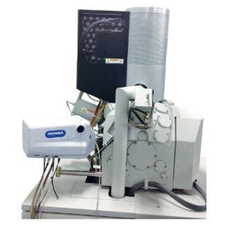
Cathodoluminescence (CL) is a nondestructive technique based on the emission of light from a material upon excitation by a high energy electron beam (or “cathode ray”). The CL detector fitted in a SEM microscope can be used as a powerful tool to characterize semiconducting materials in growth and device process development and probe:
|
|
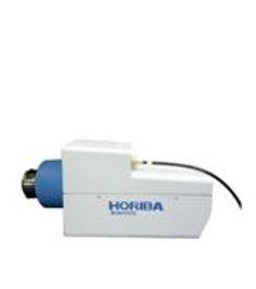
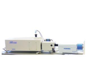
HORIBA offers CL one port-interface solutions that are compatible with all commercial SEM and FIB systems. With its wide emission energy ranging from 0.5 to 6 eV, its Raman capability, and its spatial resolution ranging from µ to nano, the Horiba CLUE systems can analyze a broad panel of semiconducting materials: group IV, II-VI, III-Vs, III-nitrides, wide band gap (SiC), 2D materials, Quantum dots, Nanowires as well as devices for optoelectronics, photovoltaics, LEDs.
 |  |  | |
| F-CLUE | H-CLUE | R-CLUE | |
| Coupling | Fiber | Direct | Fiber |
| Compatibility | All SEMs | All SEMs | All SEMs |
| Collection | Motorized Paraboloid mirror with fully retractable mechanism | ||
| Automation | Fully automated | ||
| Signal collection | ImagingCL, Spectral & Hyperspectral CL, Time-resolved CL | Imaging CL, Spectral & Hyperspectral CL, Time-resolved CL, Angular-resolved CL | Raman, PL, CL |
Do you have any questions or requests? Use this form to contact our specialists.