
Photoluminescence spectroscopy (PL) is a powerful optical method used for characterizing semiconductor materials. PL is based on shining light on sample: upon light absorption an electron-hole pair is created: an electron from the valence band jumps to the conduction band leaving a hole. The photon emitted upon recombination corresponds to the energy-difference between the valence and conduction bands and is hence lower in energy than the excitation photon. PL can be used to find:
|
|
HORIBA Scientific is a world leader in optical spectroscopy, with benefits of more than 50 years of innovation in the technique. PL characterization allows valuable insights into the properties of semiconductor materials such as group IV semiconductors, compound semiconductors, 2D materials, and their devices.
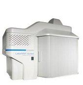 | 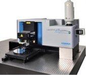 | 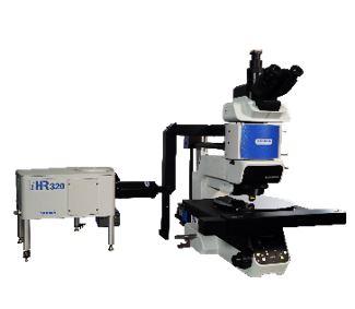 | |
| LabRAM Soleil | LabRAM Odyssey Semiconductor | SMS | |
| Wavelength range | 300-1600 nm | 200 nm-2200 nm | 250 – 14000 nm |
| Lasers | Up to 4 built in fully motorized and computer controlled | Up to 6 fully motorized | Up to 3, semi-motorized |
| Sample size acceptance | 8” | 12” | 12” |
| Detector | Open Electrode CCD, optional EMCCD, optional InGaAs arrays detector (max. 2 detectors). | Open Electrode CCD, optical EMCCD, optical inGaAs arrays detector (max. 3 detectoers). | CCD, IGA and sigle channel |
Do you have any questions or requests? Use this form to contact our specialists.