Raman analysis uses laser light scattering to reveal a material's molecular composition and structure, providing a detailed fingerprint for identification and characterization. The following sections explore what materials properties a Raman spectrum reveals, where Raman spectroscopy can be applied, and the performance characteristics that make it one of today's most versatile analytical techniques.
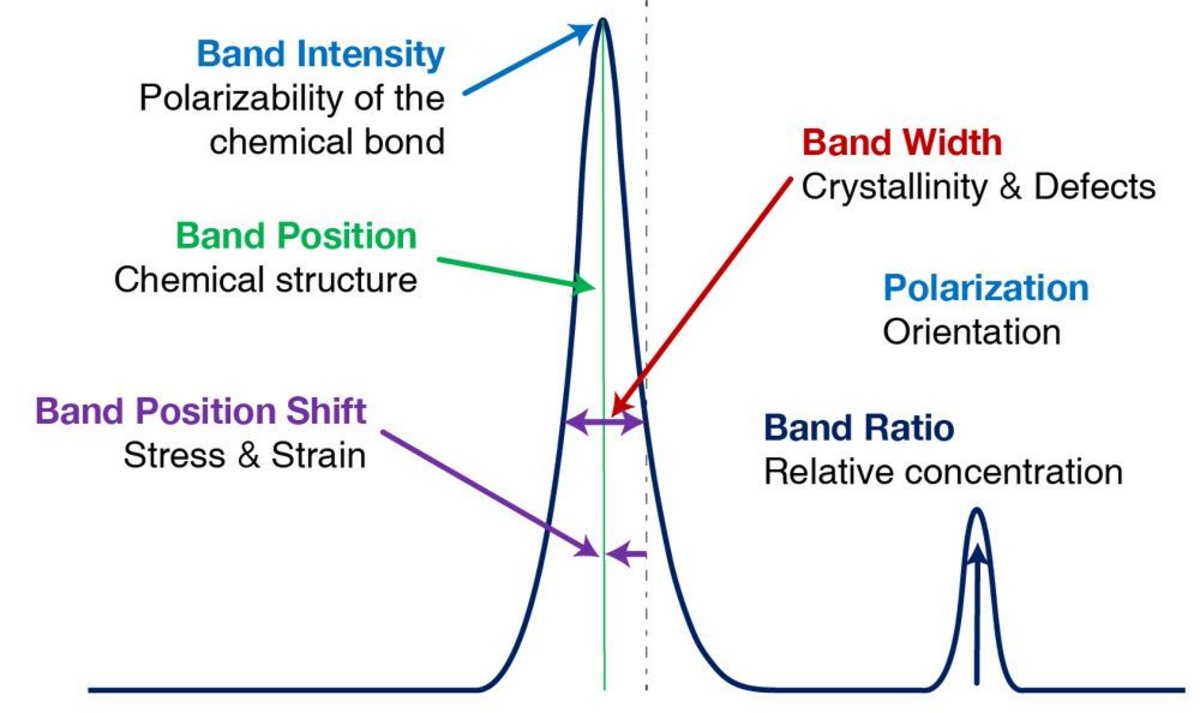
A Raman spectrum provides far more information than a simple chemical identification. It can reveal crystal structure, phase composition, crystallinity, stress, and other material properties, providing valuable insights into both composition and microstructure. Each band contains several analytical parameters that reflect the molecular composition, structure, and physical state of the sample. As illustrated in the figure, the most important characteristics are band position, intensity, width, position shift, and band ratio.
Together, these parameters transform Raman spectra into a rich source of chemical and structural information, supporting material identification, quality control, process monitoring, and advanced research.
Raman spectroscopy can also be applied in a wide range of analytical environments, from laboratory research to in situ process monitoring, in vivo measurements, and the analysis of aqueous samples.
Spectra of TiO2
In most cases Raman scattering is sensitive to material phase, polymorphism and solid form. Thus, even though two materials may have identical chemical formulae, their different crystal structure or phase will often result in distinct spectra. Phase changes are often clearly distinguished within the spectrum, but other structural differences such as polymorphism can reveal themselves only through very subtle spectral changes. In this case, it is often necessary to work with high spectral resolution to allow the minor changes to be confidently characterized.
Spectra of polycrystalline (red) and monocrystalline Si (green). Analysis of crystallinity of a material.
In most cases Raman scattering is sensitive to the degree of crystallinity in a sample. Typically a crystalline material yields a spectrum with very sharp, intense Raman peaks, while an amorphous material will show broader, less intense Raman peaks. These two states (e.g., fully amorphous, or fully crystalline) can be considered as spectral extremes, and a Raman spectrum from an intermediate state (e.g., partially crystalline) will have characteristics which are intermediate in terms of peak intensity and width (sharpness). Differences between intermediate states can be subtle, and it is often useful to have high spectral resolution capability so that minor spectral changes can be confidently characterized.
Using software peak fitting routines, it is possible to accurately calculate peak width and intensity, which can then be used, with calibration and comparison with other techniques, as a quantitative measure of crystallinity. Similar analysis of Raman maps allows images of degree of crystallinity to be produced.
Since Raman is a light scattering technique, it is possible to transfer both the laser excitation light and the Raman signal through optical fiber cables. A single cable is used to transmit the laser to the sample, while another fiber is then used to transfer the Raman signal from the sample to a standard spectrometer and detection system. These two cables are connected to a compact, rugged Raman probe head which focuses the laser onto the sample, and collects the Raman signal.
The current generation of Raman probes can be used for remote sampling hundreds of meters away from the base Raman analyzer. In addition, multiple probes can be connected to a single analyzer system, providing a cost effective method of monitoring chemical composition at multiple points within a plant.
The probes are suitable for use at high temperatures and pressures. They can operate in either an immersion mode (where the analysis head is dipped within the reaction liquid) or in a stand-off mode (where the analysis is made by focusing the laser through a transparent window in the reaction vessel or pipeline).
Remote Raman analysis can be used for:
Raman reference spectra and Raman maps of different industrial soaps.
Raman is a non-destructive, non-contact chemical analysis technique, which can be applied to in vivo analysis. Typically this is done using a compact remote Raman probe, which is coupled to the spectrometer and laser using flexible fiber optic cables.
There are many examples of in vivo analysis, particularly in the analysis of cosmetic and topical medicines on the skin. Current research is looking at the application of in vivo Raman spectroscopy in surgical environments, where it can be used as an immediate indication of tissue health.
Raman is very well suited to analysis of aqueous samples (including solutions, and biological materials such as tissue and cells). Water has a very weak Raman scattering, and typically is much weaker than other materials. Additionally the water spectrum is very simple, with only a small number of peaks, so there is minimum interference with peaks from the solute.
Thus, analysis of a solute in aqueous solution is easily possible, since in most cases the peak intensity from the solute will be stronger than those from the water, even when the water is in great excess.
Modern Raman systems further combine high sensitivity with rapid acquisition, automated workflows, and exceptional spatial resolution to enhance performance and versatility.
Raman Spectrum of Aspirin, acquisition time: 1s
The acquisition time depends on a number of factors, such as the sample itself, the desired spectral quality, and the Raman spectrometer being used. However, typical modern Raman spectrometers can acquire good quality Raman spectra in a few seconds.
Raman mapping/imaging experiments, which acquire many thousands of spectra, take longer, and typically total acquisition times for these could be in the order of a few minutes to several hours. This would depend on the number of data points being acquired, in addition to the other factors mentioned above.
MultiWell accessory for high throughput analysis
Since Raman spectroscopy is a non-contact, non-destructive technique, it can be used effectively for automated high throughput screening (HTS) and assay measurements. Typical applications include analysis of liquids/powders in multiwell plates, crystal screening, and tablet content/ uniformity assays with Transmission Raman.
High Throughput Screening (HTS) Raman systems use a combination of automated sample movement, autofocus devices, and automated data acquisition and analysis procedures to acquire spectra from hundreds of samples sequentially. HTS screening and automated measurements can even be integrated with full robot handling, removing the need for expertise and operator intervention.
Applications such as diamond like carbon (DLC) coatings for computer hard discs, and crystal and polymorph analysis in drug development now use Raman spectroscopy for automated screening, as well as many other applications which simply require routine analysis of large numbers of samples.
The laser spot size is primarily defined by the laser wavelength and microscope objective being used. The minimum achievable spot size is diffraction limited, according to the laws of physics and optics.
Laser spot diameter = 1.22 λ / NA
where λ is the wavelength of the laser, and NA is the numerical aperture of the microscope objective being used. For example, with a 532 nm laser, and a 0.90/100x objective, the theoretical spot diameter will be 721 nm.
From this equation, it can be seen that lower wavelength lasers offer higher spatial resolution (e.g., a blue laser at 488 nm will have a smaller spot size than an infra-red laser at 785 nm if the same objective is used), as do high NA objectives (e.g., a 0.90/100x objective will give a smaller spot than a 0.55/50x objective).
A slightly modified equation yields the theoretical diffraction limited spatial resolution which is achievable using an optical microscope:
Spatial resolution = 0.61 λ / NA
For a 532 nm laser with a 0.90/100x objective this would predict a spatial resolution of 361 nm. However, while this equation is applicable for standard light microscopy, the optical processes occurring during Raman microscopy are much more complex. For example, scattering of the laser/ Raman photons and interaction with interfaces in the sample can reduce this resolution. Thus, typical Raman spatial resolution is often quoted as being in the order of 1 µm, while with ‘good’ samples, spatial resolution approaching the diffraction limit can be achieved.
Certain systems, such as the LabRAM HR, can be configured with adaptive optics such as the DuoScan™ which allow laser spots to be created which can have dimensions up to 270 x 270 µm2 (depending on the objective being used).
Standard Raman microscopes are limited to spot sizes in the order of 0.5-10 µm (depending on the laser wavelength and objective being used), which is due to the optical path of the collimated laser beam through the objective. While such small spot sizes are ideal for analysis of microscopic features and offer excellent spatial resolution when combined with true confocal optics, they can be limited for bulk or macroscopic analysis.
Spatial resolution of a Raman microscope: 3D imaging of polymer laminate masking film
The achievable spatial resolution is primarily defined by the laser wavelength and microscope objective being used. The theoretical diffraction limited spatial resolution, according to the laws of physics and optics, is defined by the following equation:
Spatial resolution = 0.61 λ / NA
where λ is the wavelength of the laser, and NA is the numerical aperture of the microscope objective being used.
For a 532 nm laser with a 0.90/100x objective this would predict a spatial resolution of 361 nm. However, while this equation is applicable for standard light microscopy, the optical processes occurring during Raman microscopy are much more complex. For example, scattering of the laser/ Raman photons and interaction with interfaces in the sample can reduce this resolution. Thus, typical Raman spatial resolution is often quoted as being in the order of 1 µm, while with ‘good’ samples, spatial resolution approaching the diffraction limit can be achieved.
From this equation it can be seen that lower wavelength lasers offer higher spatial resolution (e.g., a blue laser at 488 nm will have a smaller spot size than an infra-red laser at 785 nm if the same objective is used), as do high NA objectives (e.g., a 0.90/100x objective will give a smaller spot than a 0.55/50x objective).
Spatial resolution of a Raman microscope: Raman mapping of 250 nm and 350 nm semiconductor features.
Note that the above equation relates to lateral (XY) spatial resolution. Depth (Z) spatial resolution is more complex, and depends strongly on the confocal design of the Raman microscope being used. There are several methods in use today, some truly confocal, others pseudo confocal, which work with varying success.
For a true confocal design (which incorporates a fully adjustable confocal pinhole aperture) depth resolution in the order of 1-2 µm is possible, allowing individual layers of a sample to be discretely analyzed. The achievable depth resolution will depend strongly on the laser wavelength, microscope objective, and sample structure.
Do you have any questions or requests? Use this form to contact our specialists.