Browse Products
SMS
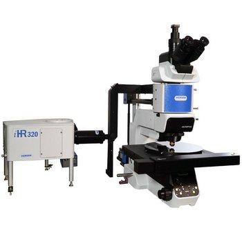
Add Spectroscopy to ANY Microscope
Take advantage of HORIBA’s full catalogue of spectrometers and sample compartments to create a custom system that allows for both macro- and micro-photoluminescence measurements in the same system! The flexibility of our imaging spectrometers allows for two independent setups on a single spectrometer.
Create a custom macro-photoluminescence system incorporating HORIBA components. A 325 nm laser is free-space coupled to a sample compartment with incorporated cryostat. The iHR320 imaging spectrometer and Syncerity CCD are used for detection.
Record time-resolved photoluminescence spectra with HORIBA’s line of optical components and TCSPC accessories. Lifetimes down to 25 ps can be measured with our DeltaDiode sources, PPD detectors, and DeltaHub electronics.
Add Spectroscopy to ANY Microscope
Sie haben Fragen oder Wünsche? Nutzen Sie dieses Formular, um mit unseren Spezialisten in Kontakt zu treten.