Nanocarbon material (diamond, graphene, carbon nanotubes and so on) have excellent electrical properties, such as high electron mobility and tolerance to a high current density. They also have high thermal conductivity and mechanical strength, and are therefore promising materials for future electronic devices for a breakthrough. HORIBA contributes its measurement technology for film thickness measurement and defects analysis of nanocarbon materials.
Film Thickness and Quality | Stress Analysis | Elemental Analysis | Foreign Object Detection/Analysis
In the advancement of thin film technology through miniaturization, we propose solutions for achieving high film deposition control, such as in-situ evaluation during the film deposition process and evaluation of thin films at the Ångström order level.
Membrane information obtained using a spectroscopic ellipsometer
We propose a multifaceted stress evaluation solution using a Raman spectrometer boasting high wavenumber and spatial resolution, along with cathodoluminescence (CL).
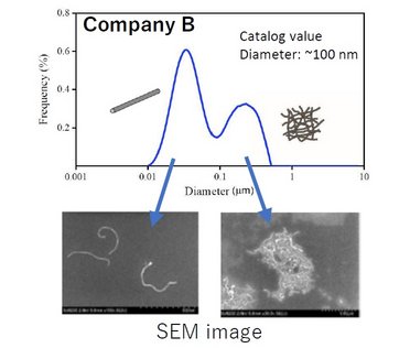
Defects in wafers can also be caused by foreign matter, and we will introduce a method of microscopic elemental analysis to identify the cause of defects.
Vous avez des questions ou des demandes ? Utilisez ce formulaire pour contacter nos spécialistes.

Spectroscopic Ellipsometer from FUV to NIR: 190 to 2100 nm
Raman Photoluminescence & Cathodoluminescence
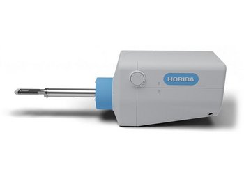
Versatile Hyperspectral Cathodoluminescence
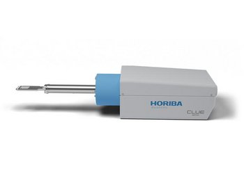
Compact Hyperspectral Cathodoluminescence

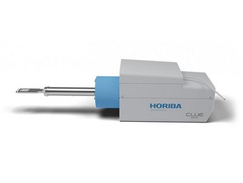
Fast Imaging Cathodoluminescence
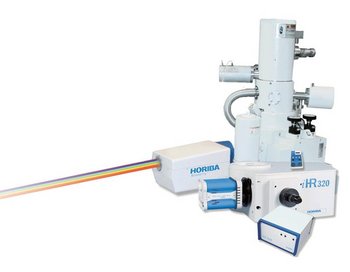
Cathodoluminescence Solutions for Electron Microscopy
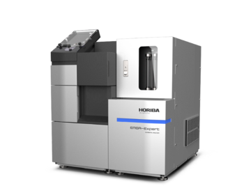
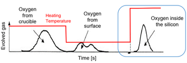
Oxygen/Nitrogen/Hydrogen Analyzer
(Flagship High-Accuracy Model)

Oxygen/Nitrogen Analyzer (Entry Model)
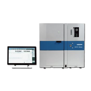
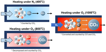
Carbon/Sulfur Analyzer (Tubular Electric Resistance Heating Furnace Model)
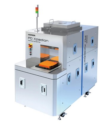
Reticle / Mask Particle Detection System