
AFM is a non-destructive scanning technique using a cantilever with a sharp tip at the end to scan over the sample surface. AFM is a tool of choice for the nanoscale characterization of semiconductor fabrication process steps. AFM offers different modes to provide:
|
|
HORIBA offers the first 100% automated system (AIST-technology) that allows for studying the topographical, electrical, and mechanical properties of traditional as well as most advanced semiconductor materials. Its design has been specially developed to be capable of being seamlessly integrated with optical spectroscopies (SNOM, Raman, Photoluminescence and TERS/SERS techniques).
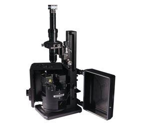 SmartSPM | |
| Automated Adjustment | Fully motorized and software-controlled laser / cantilever and photodiode alignment. |
| Optical access for upgradeability | Possible coupling to optical spectroscopies (PL & Raman) |
| Sample scanning range | 100 µm x 100 µm x 15 µm (±10 %) |
| Noise |
|
Do you have any questions or requests? Use this form to contact our specialists.