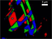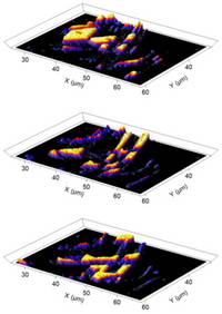

Raman remains a vital tool in the characterization of graphene materials, particularly to understand quality and layer structure.
Here, Raman imaging has been used to understand the layer structure of graphene deposited on Silicon, and illustrates mono-layer, bi-layer and tri-layer areas.
