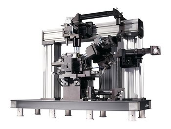
AFM

AFM-Raman Testimonials

<< Back to the AFM Optical Platform page

Read what our customers have to say...

...and discover how our AFM optical platform, coupled with Raman microscopes and spectrometers, allowed them to enhance their research and applications with co-localized AFM-Raman and TERS measurements.

Prof. Razvigor Ossikovski

NanoRaman team leader
LPICM, Ecole Polytechnique, France
A pioneer in TERS

“The nano-Raman team of LPICM lab, Ecole Polytechnique, developed jointly with HORIBA Scientific the first HORIBA TERS system prototype a dozen or so years ago. Later commercialized, the prototype featured STM and AFM SPM modes combined with side illumination in Raman backscattering configuration. Owing to its excellent performance and relative ease of use, it was applied with success to the study of various materials and nanostructures such as self-assembled organic monolayers, carbon nanotubes, patterned semiconductors, etc. Among the outstanding scientific successes achieved with the system, the world premiere demonstration of stimulated (pump - probe) TERS is to be mentioned. Being quite user-open and versatile, the prototype measurement configuration could be successfully adapted to accommodate a polarization control of both excitation and scattered radiations, an external laser pump, as well as an additional detector for Tip-Enhanced Photoluminescence.

Since the pioneering years of the TERS prototype, HORIBA Scientific have developed a novel, module-based TERS system featuring a large number of SPM modes (STM, AFM, tuning-fork, etc.) implementable under various illumination – collection conditions (off-axis, top and bottom backscattering). Thanks to the customer-oriented culture of HORIBA, the nano-Raman team of LPICM is currently updating its “historical” prototype with the novel TERS system. It will allow us not only to pursue our actual research topics by adding new measurements, but also to initiate new research areas, impossible to address with the present system.”

Prof. Dietrich R.T. Zahn

Head of the Semiconductor Physics Research Group
Technische Universität Chemnitz, Germany

A fully automated system

”With our NanoRaman instrument from HORIBA, we have the full power of Raman, AFM, TERS, TEPL, and many other related modes bundled into one system operating in reflection. Every member of my group from bachelor student level to postdoc researcher enjoys the easy usage of this fully motorized/automated system that can deliver correlated surface characterization data from microscale down to nanoscale resolution. We are using this AFM/Raman platform for research on optical and electrical properties of nanomaterials every day and we are appreciating the enormous potential of the TERS techniquefor studying nanomaterials such as CNTs and 2D TMDCs with unprecedent spatial resolution down to 2 nm.”

Prof. Masamichi Yoshimura

Head of the Surface Science Laboratory
Toyota Technological Institute, Japan

A stable and versatile solution

"We are using the NanoRaman platform from HORIBA Scientific for research on carbon-based nanomaterials and especially the characterization of graphene oxide for energy applications. This AFM/Raman system is easy-to-use with help of the state-of-art hot spot search function and has number of unique build-in SPM techniques, including a unique imaging mode that makes TERS possible. HORIBA (and former AIST-NT) has developed one of the most stable and versatile scanning probe microscope for the combination with Raman spectroscopy. With the clever, fully motorized and automated instrument alignment, every advanced measurement at the nanoscale become an easy to configure experiment."

Dr Ivan T. Lucas and Prof. Emmanuel Maisonhaute

Laboratory "Interfaces and Electrochemical Systems"
Sorbonne University, France

Great technical support

“We have been working for two years on a versatile configuration of the NanoRaman platform from HORIBA that allows both reflection and transmission measurements. As researchers in an electrochemistry Lab, we were searching for analytical tools which enable the characterization of materials at the nanoscale and under the condition of their operation. The stability of the SPM system (true atomic/molecular resolution) and the robustness of the optical coupling, which enables fast and effective TERS mappings, totally met our expectations. The versatility of the HORIBA system already made possible new characterization pathways such as TERS in liquid and electrochemical TERS. We have also greatly enjoyed the technical assistance from HORIBA which has definitively boosted our instrumental developments”.

Browse Products

OmegaScope
OmegaScope

The AFM optical platform

SmartSPM
SmartSPM

Advanced stand-alone AFM

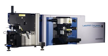
LabRAM Odyssey Nano
LabRAM Odyssey Nano

AFM-Raman for physical and chemical imaging

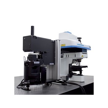
XploRA Nano
XploRA Nano

AFM-Raman for Physical and Chemical imaging

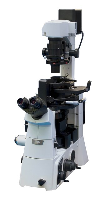
CombiScope
CombiScope

AFM and inverted light microscopy

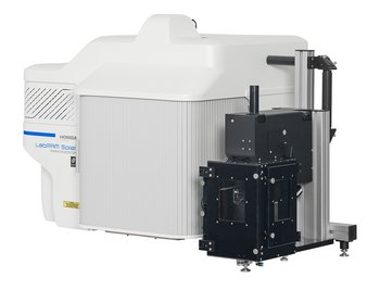
LabRAM Soleil Nano
LabRAM Soleil Nano

Real-time and Direct Correlative Nanoscopy

TRIOS
TRIOS

Versatile AFM Optical Coupling

Request for Information

Do you have any questions or requests? Use this form to contact our specialists.

* These fields are mandatory.

Corporate