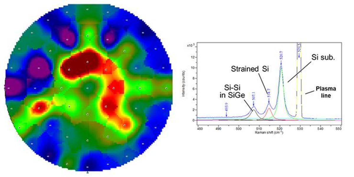
Group IV elements (Si, Ge) have been historically used in the semiconductor industry, especially in the manufacture of planar and, more recently, three-dimensional (3D) structures (FinFET, Nanosheet FET, Gate-all-Around FET). Manufacturing processes are becoming more and more complex, and such complexity drives an evolution in characterization providing extensive information about material properties (stress measurements, crystallinity, phase extraction) allowing process stabilization at the R&D stage.
Application: 2D/3D transistors, photovoltaics
Materials: Si, Ge, SiGe
Raman image of a silicon chip with crystalline, poly and amorphous silicon region
Stress distribution map derived from Raman data of a strained silicon layer on SiGe; Representative Raman spectrum
Photoluminescence and Raman Wafer Imaging
如您有任何疑問,请在此留下詳細需求或問題,我們將竭誠您服務。

