尺寸
1.42
MB
PLATO Series Brochure
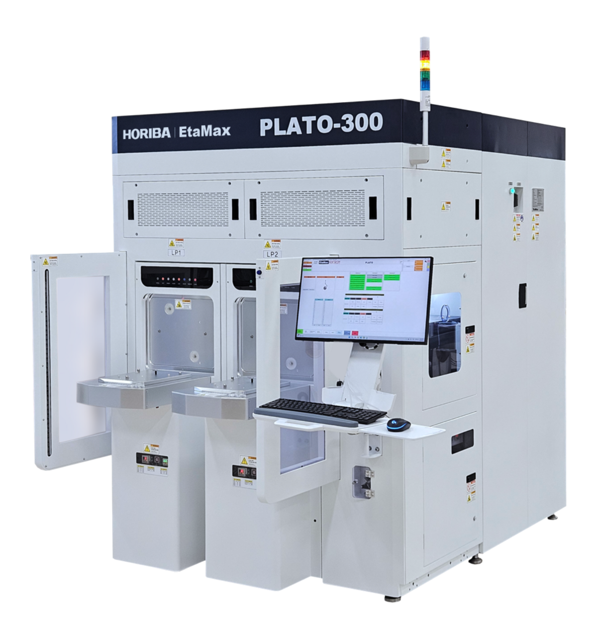
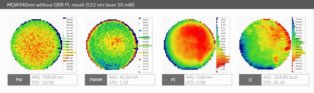
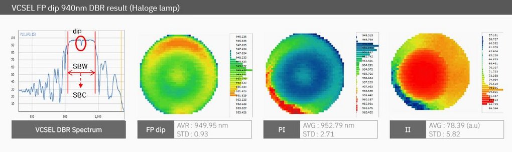
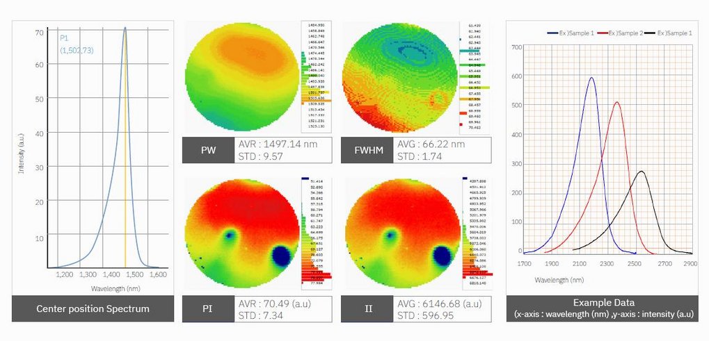
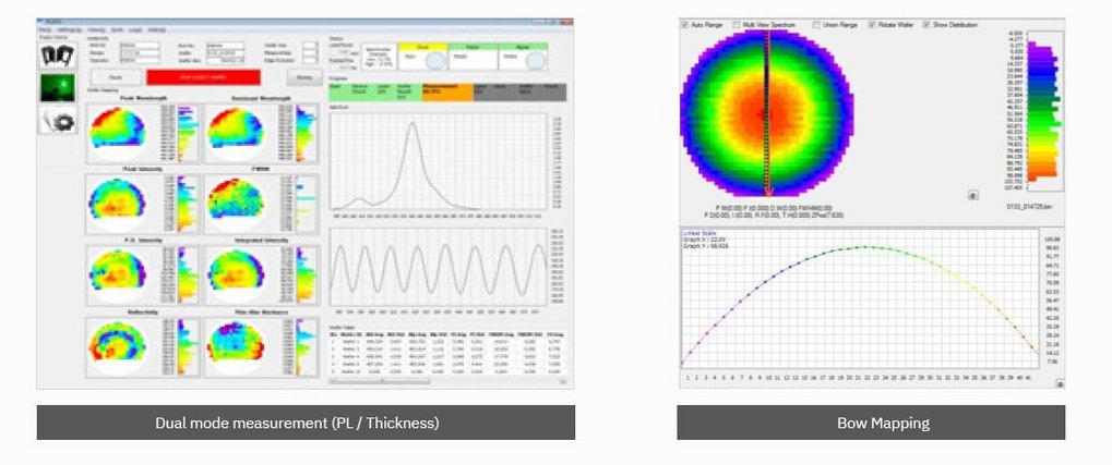
Automatic Photoluminescence Mapping System
Automatic Photoluminescence Mapping System
Automatic Photoluminescence Mapping System
Automatic Photoluminescence Mapping System
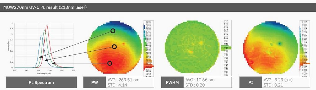
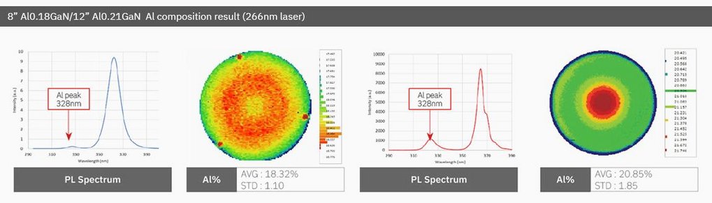
| Light source | UV | 213nm, 266nm, 325nm |
|---|---|---|
| VIS | 375nm, 405nm, 532nm | |
| NIR | 980nm, 1064nm | |
| Measurement Item | DBR Measurement | Visible range, NIR range |
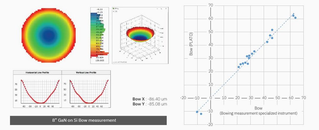
| Bow Measurement | 10~1000um | |
| Laser Marking | CE-CoC, CE-DoC, KCs, S-Mark | Sapphire, Si, GaAs |
| Wafer Transfer | Robot type | Single-arm, Dual-arm |
| Cassette mapping sensor | ||
| Wafer size | SEMI standard 2”, 3”, 4”, 6”, 8”, 12” | |
| Cassette type | Open Cassette, SMIF, FOUP | |
| Identification | Wafer ID reader, Cassette ID reader | |
| Certification | CE-CoC, CE-DoC, KCs, S-Mark | |
| Etc. | SECS/GEM | |
如您有任何疑問,请在此留下詳細需求或問題,我們將竭誠您服務。