
AFM-Raman system combines both atomic force microscopy (AFM) and optical spectroscopy to deliver colocalized physical and chemical data. With the use of a plasmonic metal coated AFM probe, both data can be collected with nanoscale spatial resolution and is the best suited for the characterization of emerging 2D semiconductor materials and devices. Comprehensive analysis is accessible with the acquisition of the following correlated information:
|
|
For over 15 years, HORIBA has provided TERS-proven systems with the most user-friendly and robust technology integrating AFM modes with optical spectroscopies for the deployment of most advanced semiconductor materials.
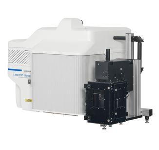 | 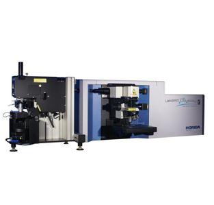 | ||
| LabRAM Soleil Nano | LabRAM Odyssey Nano | ||
| User Ergonomy | Piezo adjustment of objective for robust and accurate probe/spectroscopy laser alignment | ||
| Wavelength range | 300-1600 nm | 200 nm-2200 nm | |
| Standard wavenumber cut-off | < 30cm-1 | < 50cm-1 | |
| Lasers | Up to 4 built in fully motorized and computer controlled | Up to 6 fully motorized | |
Do you have any questions or requests? Use this form to contact our specialists.
