
Raman spectroscopy is a non-destructive chemical analysis technique that uses inelastic scattering of light to study the vibrational modes in a sample. Raman spectroscopy provides detailed information used in the semiconductor industry to optimize R&D processes and improve device yield:
|
|
HORIBA Scientific is the world leader in Raman spectroscopy, with benefits of more than 50 years of innovation in the technique. Raman characterization allows valuable insights into the properties of semiconductor materials such as group IV semiconductors, compound semiconductors, 2D materials, and their devices.
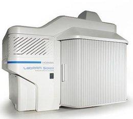 | 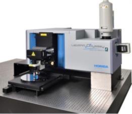 | |
| LabRAM Soleil | LabRAM Odyssey Semiconductor | |
| Wavelength range | 300-1600 nm | 200 nm-2200 nm |
| Motorized stage | 75 mm x 50 mm or 120 mm x 80 mm | 300 mm x 300 mm |
| Lasers | Up to 4 built-in fully motorized and computer controlled | Up to 6 fully motorized |
| Spectral resolution (785 nm excitation wavelength with 1800 gr/mm grating) | ≤ 0.9 cm-1 | ≤ 0.2 cm-1 |
| Spectral stability RMS (measured on Si 520 cm-1 line) | < 0.02 cm-1 | < 0.02 cm-1 |
Do you have any questions or requests? Use this form to contact our specialists.
