


PDF
3.92
MB

Application Overview
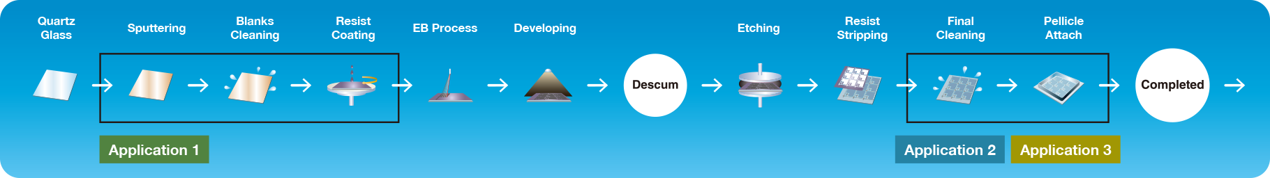
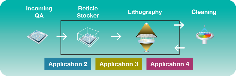
Semiconductor : Mask / Lithography Process

Photolithography, also called optical lithography or UV lithography, is a process used in microfabrication to pattern parts on a thin film or the bulk of a substrate (also called a wafer). It uses light to transfer a geometric pattern from a photomask (also called an optical mask) to a photosensitive (that is, light-sensitive) chemical photoresist on the substrate. A series of chemical treatments then either etches the exposure pattern into the material or enables deposition of a new material in the desired pattern upon the material underneath the photoresist. In complex integrated circuits, a CMOS wafer may go through the photolithographic cycle as many as 50 times.
Photolithography shares some fundamental principles with photography in that the pattern in the photoresist etching is created by exposing it to light, either directly (without using a mask) or with a projected image using a photomask. This procedure is comparable to a high precision version of the method used to make printed circuit boards. Subsequent stages in the process have more in common with etching than with lithographic printing. This method can create extremely small patterns, down to a few tens of nanometers in size. It provides precise control of the shape and size of the objects it creates and can create patterns over an entire surface cost-effectively. Its main disadvantages are that it requires a flat substrate to start with, it is not very effective at creating shapes that are not flat, and it can require extremely clean operating conditions. Photolithography is the standard method of printed circuit board (PCB) and microprocessor fabrication. Directed self-assembly is being evaluated as an alternative to photolithography.
Photolithography is commonly used to produce computer chips. When producing computer chips, the substrate material is a resist covered wafer of silicon. This process allows hundreds of chips to be simultaneously built on a single silicon wafer.
Do you have any questions or requests? Use this form to contact our specialists.