



Fully Automated Thin Film Inspection System Xtrology
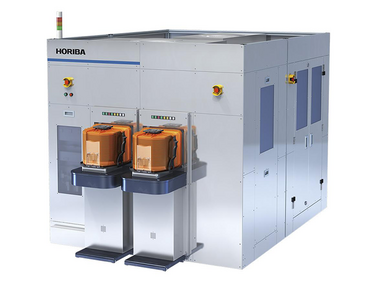
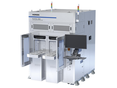
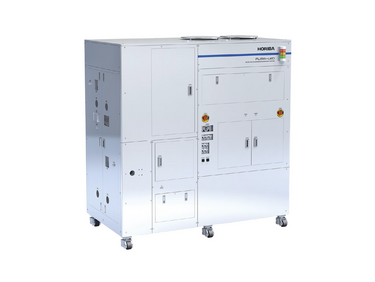
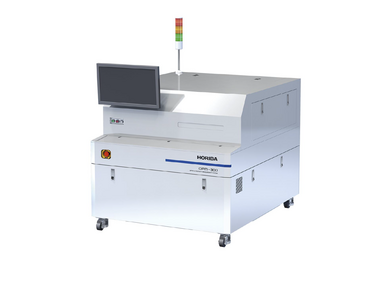
HORIBA has combined its analytical and measurement technologies with fully automated measurement technology to develop imaging-capable measurement systems with automatic transport. These systems provide key wafer parameters in a timely manner, such as film thickness, crystallinity, defects, and particle detection.
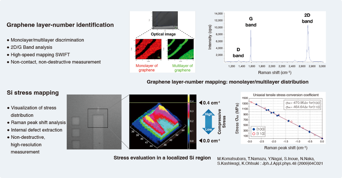
Xtrology, Fully Automated Thin-film Inspection System, automatically evaluates thin-film materials. Built around HORIBA’s proprietary Raman spectroscopy technology, it enables quantitative, non-destructive, non-contact analysis of layer count, crystallinity, stress, and defects. It provides high-precision evaluation of a wide range of materials, from graphene and other two-dimensional materials to Si/SiC devices. With the high-speed mapping technology SWIFT, it can measure large areas quickly and densely, supporting material evaluation and process development from R&D to mass production.
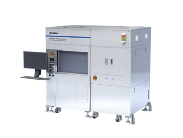
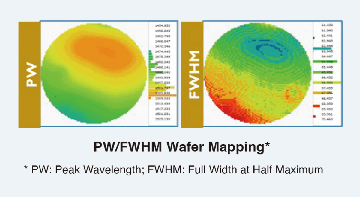
The PLATO Series, Photoluminescence Mapping System, is a compound-semiconductor material characterization system based on photoluminescence (PL) technology. Depending on the excitation laser and spectroscopic method selected, it can measure spectral characteristics from DUV to NIR. It supports 2- to 12-inch wafers, and the lineup includes an auto-loading model for automated handling. By analyzing parameters such as peak wavelength, intensity, film thickness, and wafer warpage, the system helps improve yield.
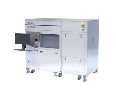
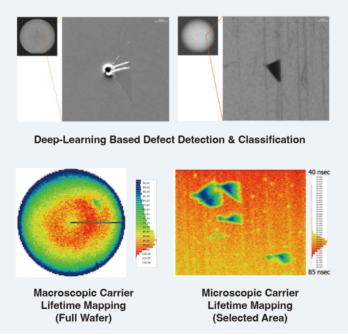
MiPLATO-SiC, the SiC Wafer Defect Inspection System, is a PL mapping system optimized for SiC wafers. Utilizing a spiral mapping method, it acquires microscopic PL images of the entire wafer in a short time. Through real-time data analysis using deep learning capabilities, it creates maps of defect distribution and density, enabling the prediction of yield during device fabrication. Our patented automatic navigation function allows for accurate classification of all stacking faults through wavelength analysis. Furthermore, based on precise location information derived from the defect map, it is possible to perform micro-mapping of carrier lifetime and spectral characteristics in specific regions, as well as macro-mapping across the entire wafer.