The industrialization of 2D materials and their emergence in electronic devices will not only depend on the uniformity assessment of their deposition on large wafers but also on overcoming the presence of defects which reduces the size of high-quality crystals, and on preserving quality through the processing steps.
Application: CMOS, electrodes, barriers
Materials: Graphene, Transition Metal Dichalcogenides, Hexagonal Boron Nitride (h-BN)
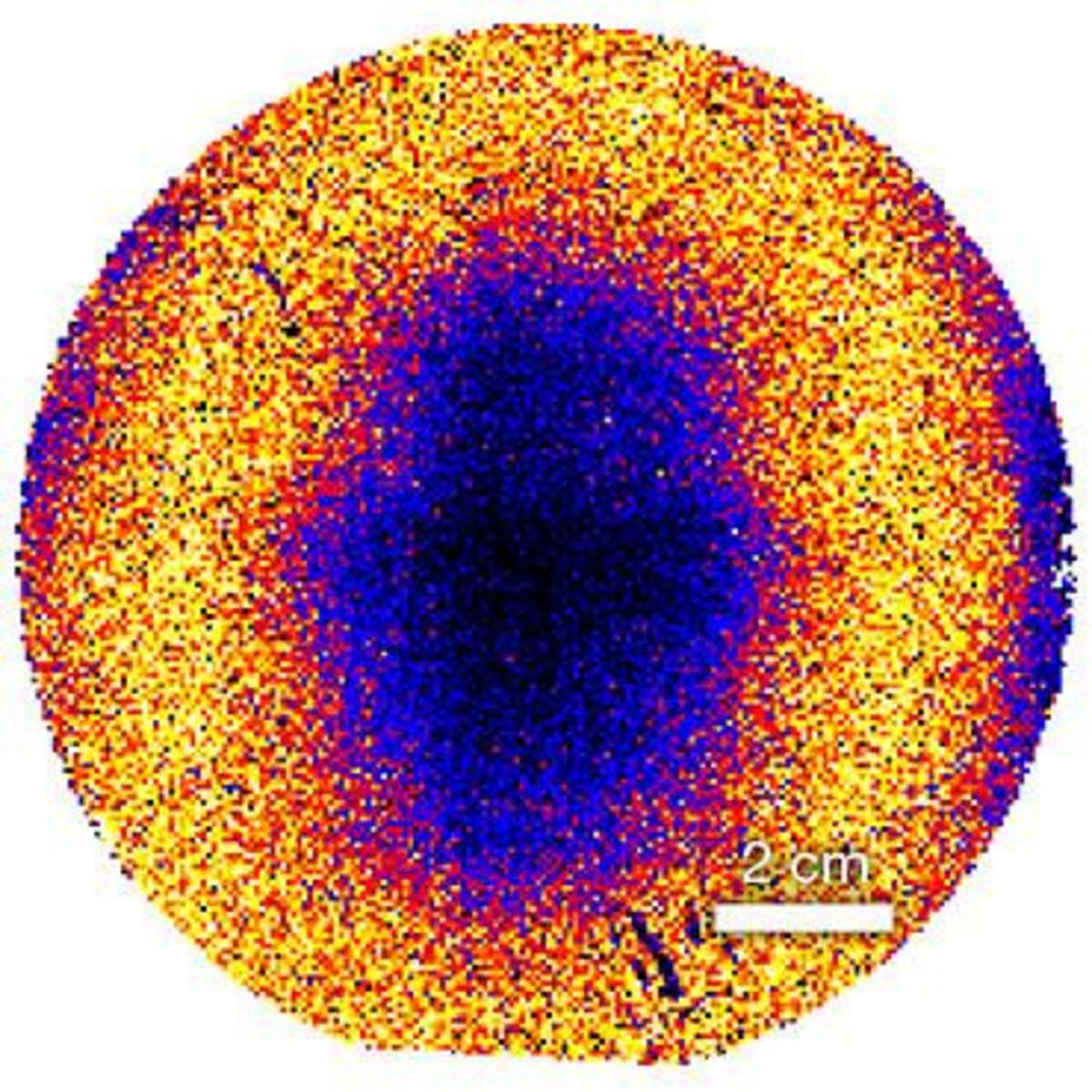
Graphene Raman image of a 4" wafer
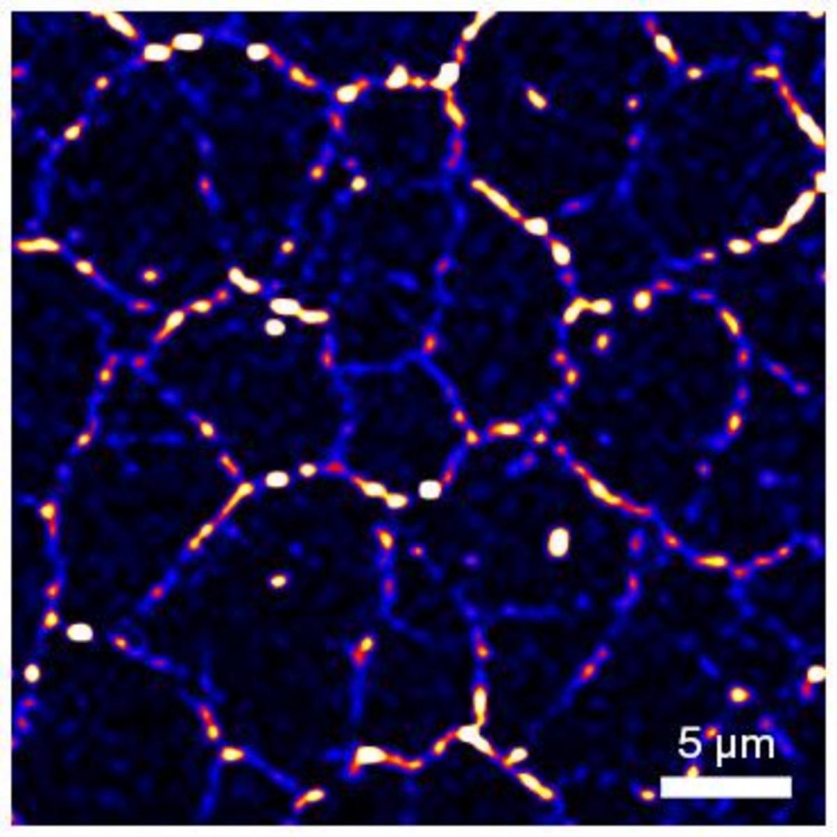
High resolution Raman image on defects
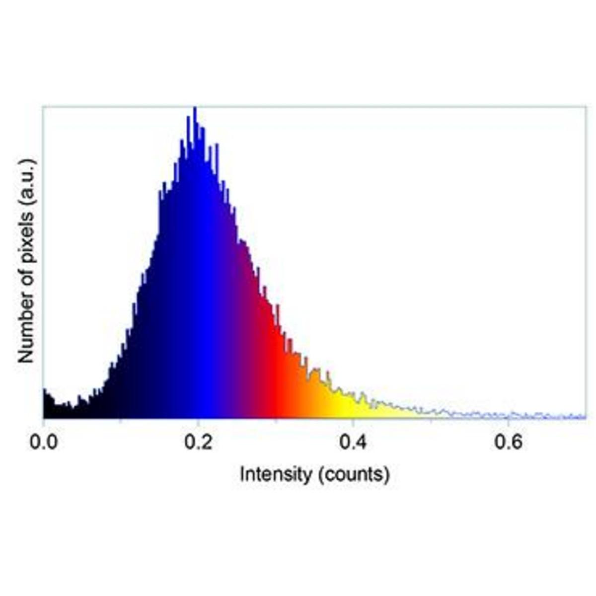
D/G distribution peak analysis
Photoluminescence and Raman Wafer Imaging
У вас есть вопросы или пожелания? Используйте эту форму, чтобы связаться с нашими специалистами.


