Compound semiconductors enable the production of advanced power devices and active photonic devices such as light sources and detectors. Successful fabrication of such devices relies on the high quality of the underlying materials (SiC, AlGaN, GaN, GaAs, InGaAs etc.) and precise deposition of intended geometries on a wafer substrate.
Defects in materials such as imperfections in geometries, adversely affect yield and usually increase cost and development times of compound semiconductor devices
Application: Displays, LEDs, laser diodes, quantum wells
Materials: GaAs, InGaAs, InP, InGaN, GaP
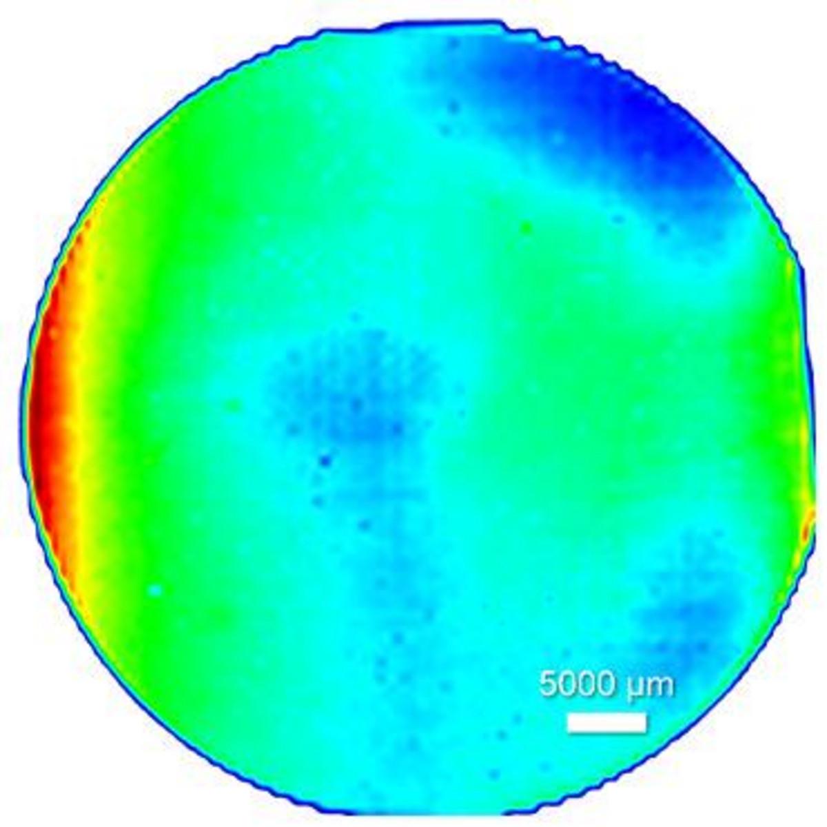
PL image of GaAs wafer showing inhomogeneities
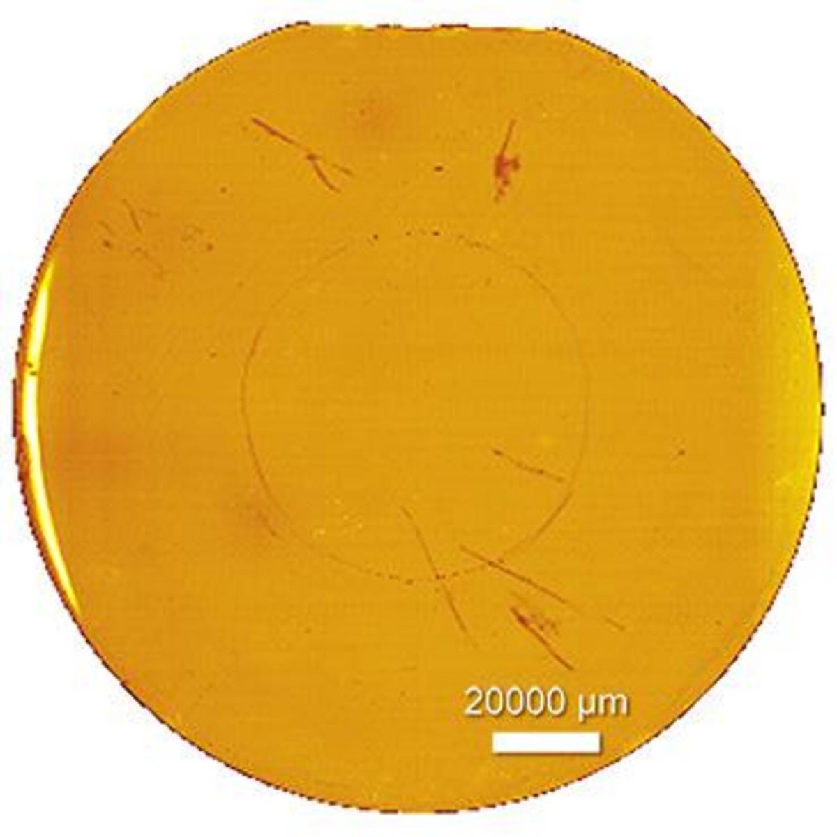
PL image of an InGaAs based multiquantum well structure
PL image of InGaAsP layer on InP-based wafer showing inhomogeneities
Application: Power devices
Materials: Gallium nitride (GaN), Silicon Carbide (SiC), Gallium Oxide (Ga2O3)
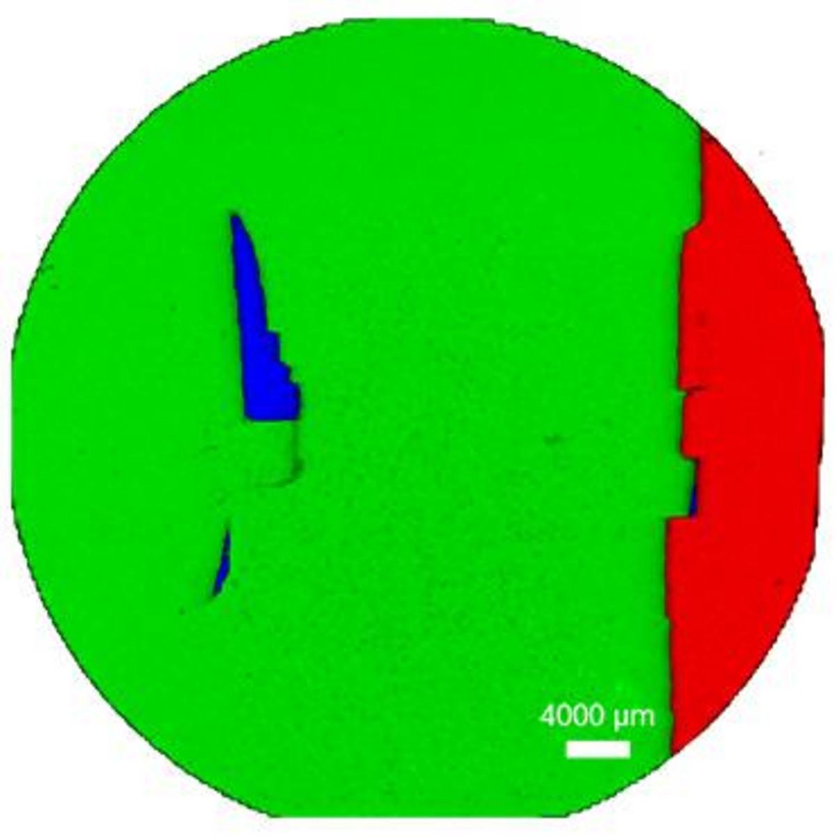
Raman image of SiC wafer showing different crystalline forms
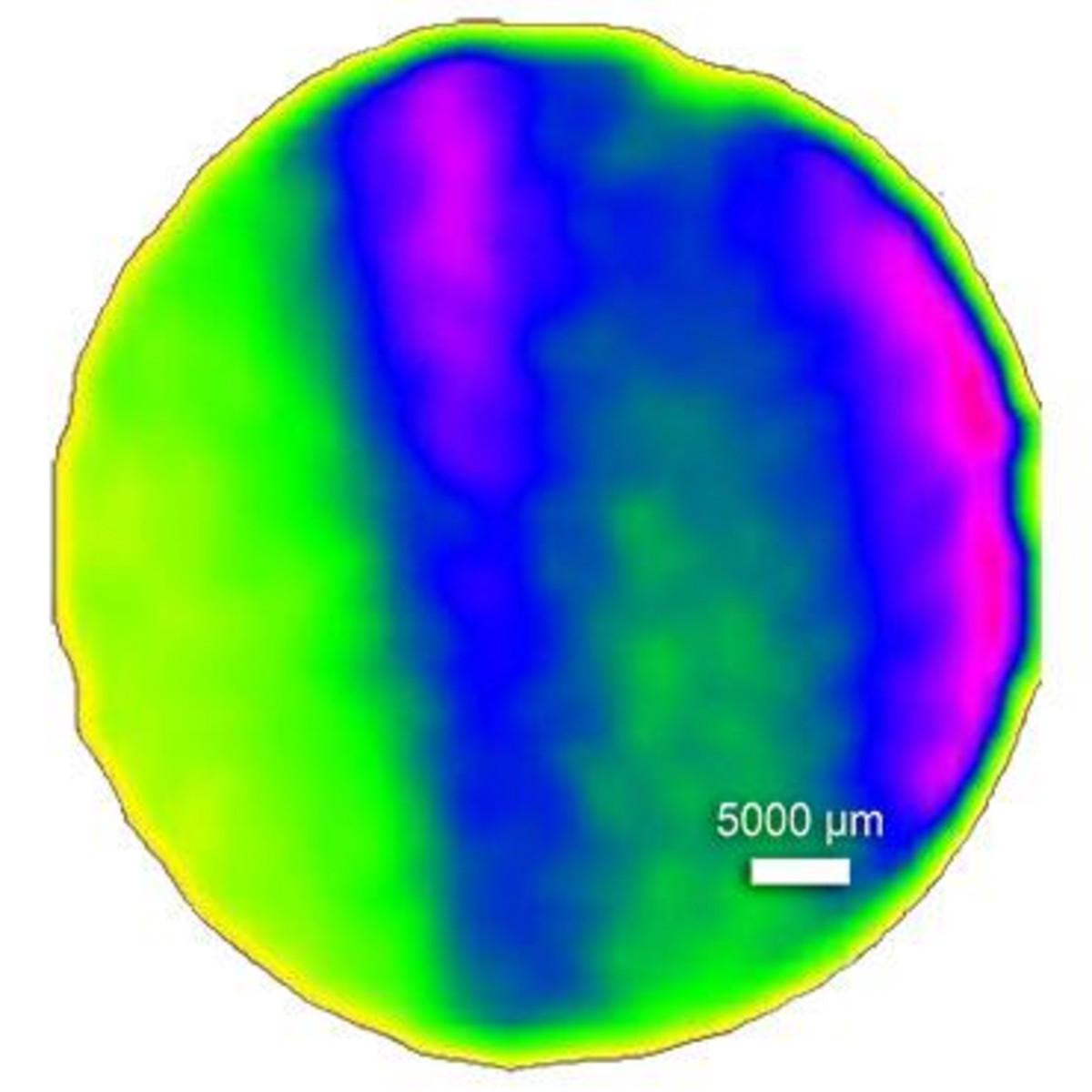
Raman image of doping distribution across a SiC wafer
Photoluminescence and Raman Wafer Imaging
У вас есть вопросы или пожелания? Используйте эту форму, чтобы связаться с нашими специалистами.


