PDF
2.05
MB

Micro-XRF analysis for the Electronics Industry

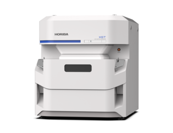
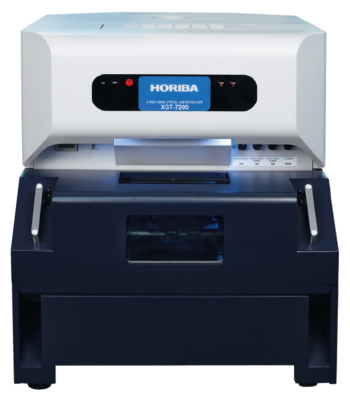
The combination of the XGT-5000’s ground breaking spatial resolution and sensitivity means it is the instrument of choice for fast analysis of electronic components, whether for analysis of restricted harmful elements (the WEEE/RoHS ‘lead free’ legislation), trouble shooting, or R&D. With a beam size of 10 µm even the smallest features on a populated circuit board can be accurately analysed, allowing microscopic contaminants to be identified, wiring/soldering defects to be located, and elemental composition of parts and components to be checked. In addition, the capability for simultaneous XRF and transmission x-ray mapping allows information to be obtained on parts not visible to the eye, for example, circuitry encased in plastic.
У вас есть вопросы или пожелания? Используйте эту форму, чтобы связаться с нашими специалистами.