Depth Profile Analysis of Thin Multilayers with nanometric resolution by Glow Discharge Optical Emission Spectroscopy (GD-OES)This application note demonstrates the use of pulsed RF GD-OES for nanometric depth profiling of (Al,Ga)N quantum wells and quantum dots. The technique supports process optimization and quality control of layer thickness and composition in advanced UV optoelectronic structures.
Spectroscopic characterization and detection of yield-killing defects in micro-LED wafersEmerging display technologies demand high brightness, low power consumption and longer lifetime. Arrays, of self-emitting, micron-sized LEDs or Micro-LED (µLED), are considered a strong contender to replace current OLED or LCD displays.
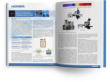
Micro-Photoluminescence Mapping and Identification of Yield-Killing Defects in 4H-SiCThis application note demonstrates how deep-UV optimized HORIBA multimodal SMS can be applied to characterize PVT-grown 4H-SiC substrates, as well as epitaxial 4H-SiC structures.
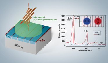
How Raman Spectroscopy can measure nanoelectronics structuresRaman spectroscopy is an essential tool for the characterization of semiconductors. However, Raman spectroscopy's spatial resolution is limited by the diffraction limit to about 200-300 nanometers, which can be insufficient for analyzing the increasingly smaller features of modern electronic devices.
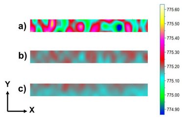
利用拉曼光谱监测4H-SiC的亚表面应力拉曼光谱可对4H-SiC半导体进行非破坏性应力分析。本研究展示了拉曼光谱峰位移可以区分不同表面处理工艺(如切割、研磨和CMP抛光)之间的差异,可用于电子学领域的工艺优化与质量控制。
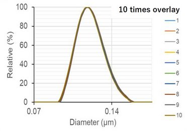
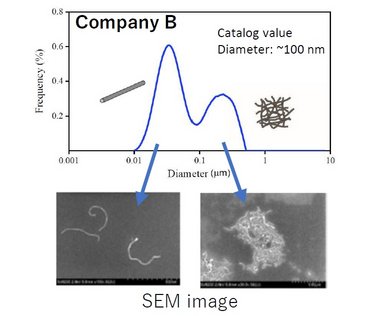
碳纳米管的直径(厚度)分布与分散/聚集状态的表征碳纳米管(CNTs)是一种完全由碳原子组成的薄、轻、柔性的弦状材料。CNTs容易聚集,因此了解和控制其聚集状态是达到预期性能的关键。为此,需要一种能够快速评估从孤立分散到聚集的宽粒径分布(PSD)的高分辨率分析方法。 本文使用 Partica CENTRIFUGE 离心式纳米粒度分析仪,对三家公司的四种碳纳米管进行了测量。表明了分析仪的颗粒表征能力,将有助于碳纳米管的性能评估和质量控制。
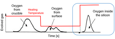
硅片中氧的定量分析硅片中氧的浓度对硅片的电阻有很大影响。因此,即使硅片中仅含有极少量的氧,对其浓度的控制也是至关重要的。然而,在分析高掺杂单晶硅时出现了一个挑战,由于其独特的性质和高掺杂水平,分析这些样品中的氧变得非常困难,杂质和掺杂剂的存在会干扰使用 FT-IR 光谱法对氧浓度的精确测量。