
Optical Emission Spectroscopy (OES) is a very flexible method which measure the amplitude or amplitude-ratio changes of particular emission lines emitted by a plasma. Because it is a rich real-time source of information for plasma etch and deposition monitoring, OES has been used for years by the Semiconductor industry. In addition to Endpoint monitoring, OES is used for detailed diagnostics such as tool fluctuations, tool-to-tool variations, and tool/ process variations after routine chamber maintenance or repair by means of plasma process-spectra matching.
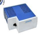
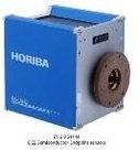
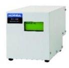
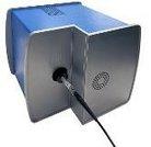
Depending on the application, HORIBA offer a wide range of OES spectrometer and Advanced Process Control solution package to meet the needs of the final end-user or tool manufacturer.
| VS70 | EV2.0 | EV-140C | OES-Star | M116 | VU90 | |
 |  |  |  | 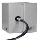 | 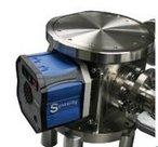 | |
| Spectral range | 200-910nm | 200-1050nm | 200-800nm | 200-1050nm | 185-1050nm | 115-320nm |
| Resolution | < 2 nm | < 2 nm | < 2 nm | < 1 nm | < 1.3 nm | < 0.75 nm |
| Optical Coupling to the chamber | Optical Fiber | DN25 Flange or Optical Fiber | Optical Fiber | Optical Fiber | Optical Fiber | Direct |
| Communication with the tool | Ethernet EtherCAD USB | TCPIP | TCPIP | USB | USB | USB |
| Software | LabView | SigmaP | SigmaP | LabView | LabView | LabView |
Sie haben Fragen oder Wünsche? Nutzen Sie dieses Formular, um mit unseren Spezialisten in Kontakt zu treten.