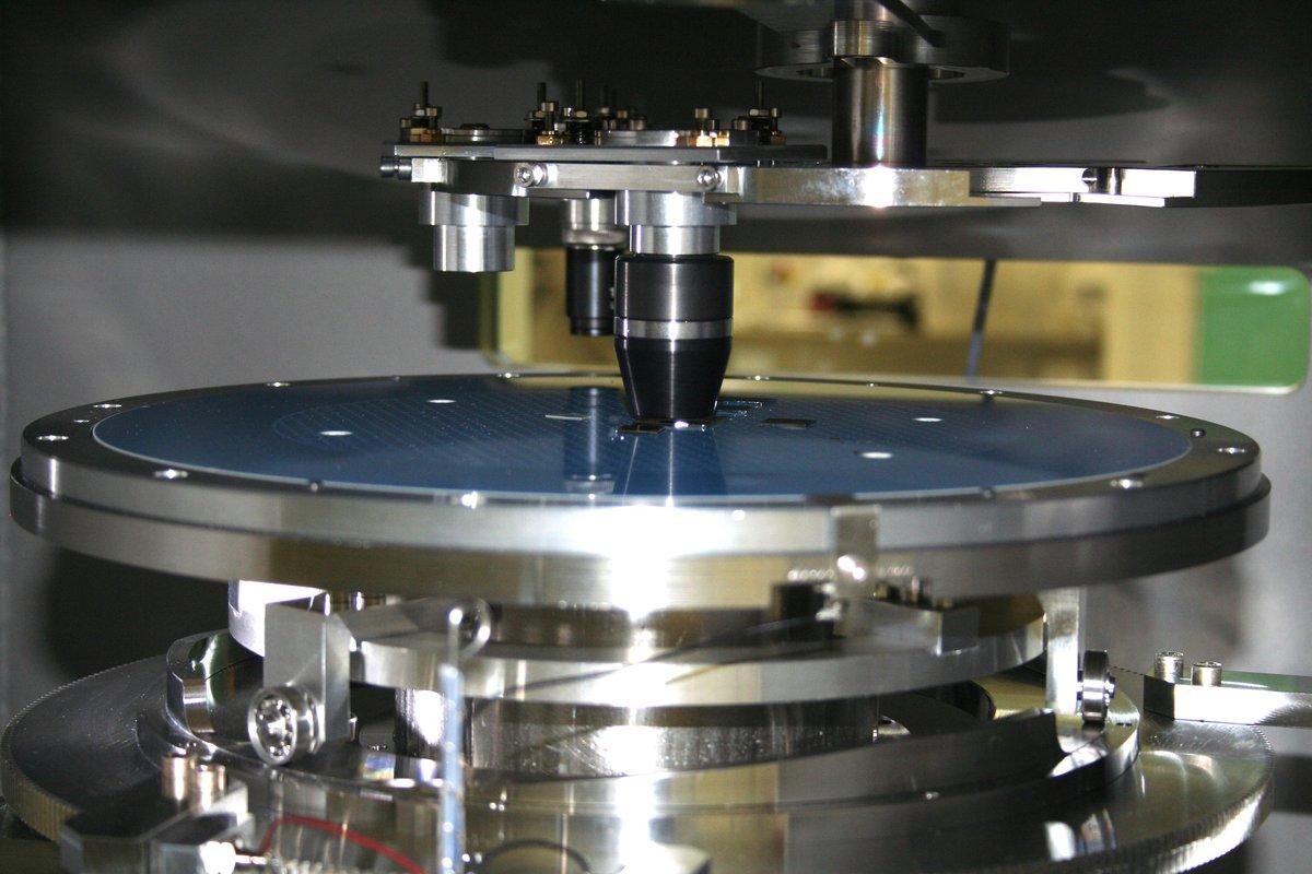
Semiconductor Wafer Handling

Raman Accessory for Imaging

HORIBA Scientific can offer new large area sample stages suitable for the translation and mapping of large 8 inch semicon wafers.

Segment: Scientific
Manufacturing Company: HORIBA France SAS

Available in manual or motorized formats and for standard and cleanroom environments the stages provide a precise, stable and robust translation of previously difficult to handle large area wafers and similar such samples.

The motorized version offer the ability for large area mapping, ideal for PL and Raman characterization of complete semiconductor wafers.

The large area stages are ideally matched to the FSM or dual microscope version of the LabRAM Odyssey, Raman/PL microscopes.

Request for Information

Do you have any questions or requests? Use this form to contact our specialists.

* These fields are mandatory.

Corporate