Multimodal spectroscopic metrology, integrating Photoluminescence (PL), Time-Resolved Photoluminescence (TRPL), and Raman spectroscopy, is a rapid, non-destructive, and high-resolution technique for comprehensively characterizing micro-LED mu (LED) epitaxial wafers. This approach provides atomic-level insights to monitor epitaxial growth quality and detect yield-killing microscopic defects that directly impact display brightness, color uniformity, and pixel functionality.
Electronic Device Failure Analysis (EDFA) recently published an article on this topic, titled Spectroscopic Characterization and Detection of Yield-Killing Defects in Micro-LED Wafers. The publication highlights how advanced metrology tools, specifically HORIBA's LabRAM Odyssey and SMS320 systems, enable the simultaneous optical characterization of wafers to identify structural imperfections like micro-pits and micro-cracks. Specifically, the article demonstrates the effectiveness of high-resolution PL and Raman spectroscopy in assessing residual stress and carrier lifetimes, offering a robust approach for ensuring die yield in the mass production of next-generation displays.
Read the full story on the ASM International website to explore the data and methodology. https://static.asminternational.org/edfa/202508/16/
The transition from OLED and LCD to micro-LED technology is driven by the demand for higher brightness and lower power consumption in devices like smartwatches and augmented reality (AR) glasses.
To achieve the high pixel densities required for these applications, microLEDs must be fabricated with dimensions of 3 μm or smaller. At this scale, even microscopic defects in the epitaxial wafer can lead to dead pixels or uneven color. With the mu LED display market projected to reach USD 21 billion by 2028, early-stage identification of these defects is financially critical to maintain high production yields and lower manufacturing costs.
The study utilizes a multimodal approach to fully characterize the material properties:
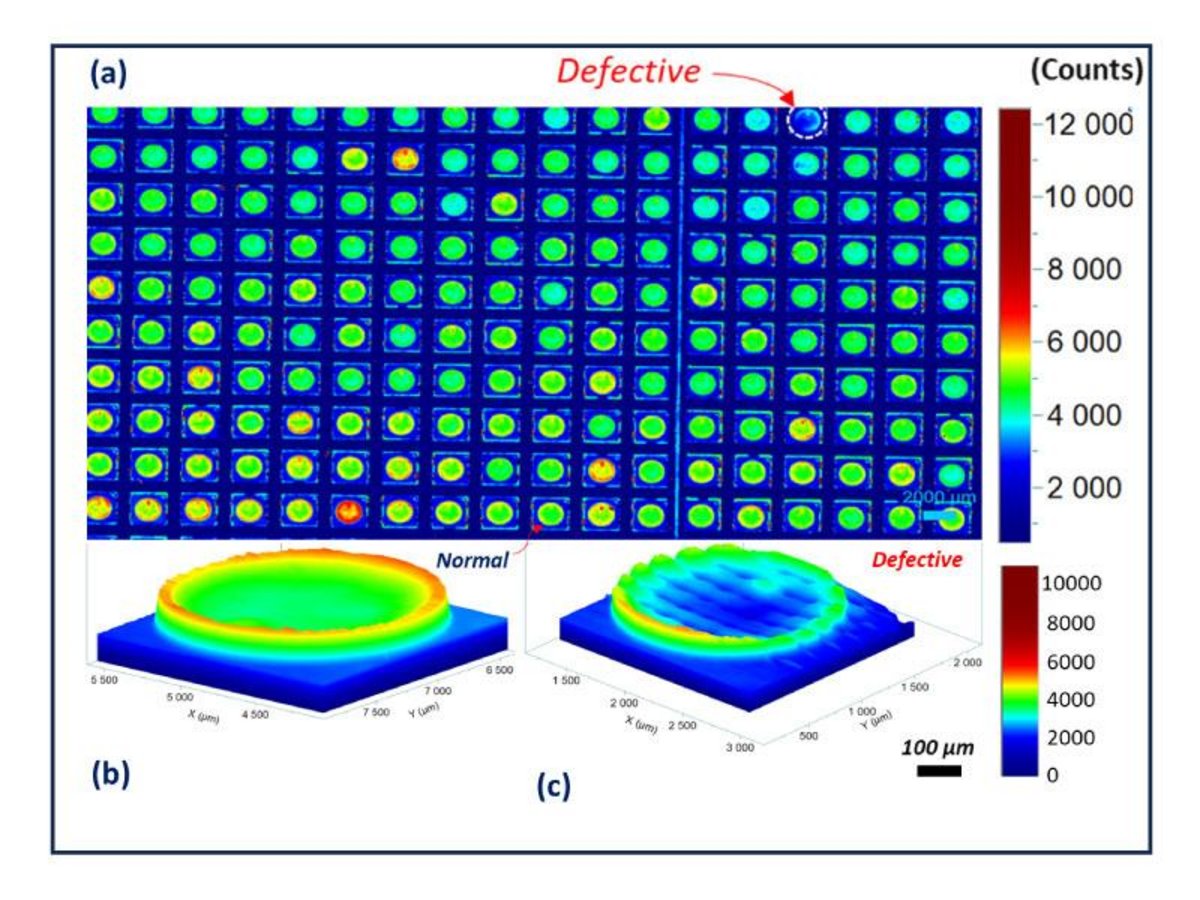
Defects present themselves through distinct optical signatures compared to non-defective regions:
The resolution is adjusted based on the scale of the inspection:
Do you have any questions or requests? Use this form to contact our specialists.
