
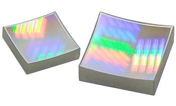
Photoluminescence spectroscopy, often referred to as PL, is when light energy, or photons, stimulate the emission of a photon from any matter. It is a non-contact, nondestructive method of probing materials. In essence, light is directed onto a sample, where it is absorbed and where a process called photo-excitation can occur. The photo-excitation causes the material to jump to a higher electronic state, and will then release energy, (photons) as it relaxes and returns to back to a lower energy level. The emission of light or luminescence through this process is photoluminescence, PL.
Our PL optimized series of spectrophotometers are used in Fluorescence Spectrometers, Raman Spectrometers and our Custom Optical Solution Systems. These products are also making a major contribution to the development of nanomaterials, semiconductors, photovoltaics / solar cells.
By combining Raman analysis with PL detection, it is possible to characterize both the vibrational and electronic properties of materials on a single bench top platform. Combined Raman-PL systems allow confocal mapping capabilities with sub-micron spatial resolution. A wide range of excitation wavelengths is possible, from the UV to NIR, allowing control of the penetration depth into the material, and thus, control of the volume sampled.
Photoluminescence used in Fluorescence spectroscopy can provide two results: Fluorescence and Phosphorescence. The Photoluminescence quantum yield or PLQY of a molecule or material is defined as the number of photons emitted, as a fraction of the number of photons absorbed is one of the common techniques for Fluorescence Spectroscopy.
Photoluminescence is when light energy, or photons, stimulate the emission of a photon. It takes on three forms: fluorescence, phosphorescence and chemiluminescence. Fluorescence is a type of luminescence caused by photons exciting a molecule, raising it to an electronic excited state. The excited state undergoes rapid thermal energy loss to the environment through vibrations, and then a photon is emitted from the lowest-lying singlet excited state. This process of photon emission competes for other non-radiative processes including energy transfer and heat loss.
Time resolved photoluminescence (TRPL) can be performed with spectrometers and microscopes. Using Time Correlated Single Photon Counting (TCSPC) the instruments with Picosecond lasers for excitation sources has been used in the solar cell industry to monitor carrier lifetime and cell performance.
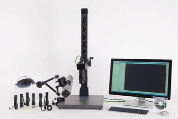
Add Spectroscopy to ANY Microscope
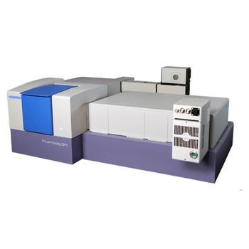
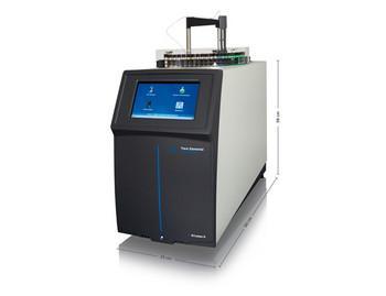
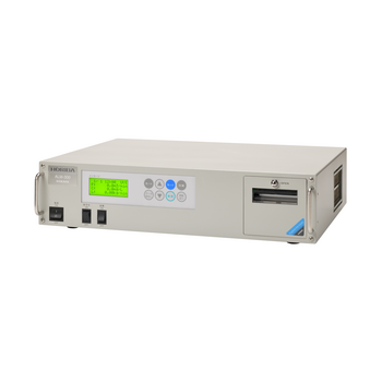
Fluorescence and Absorbance Spectrometer
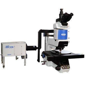
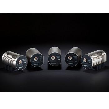
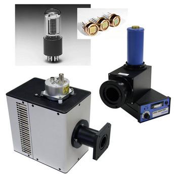
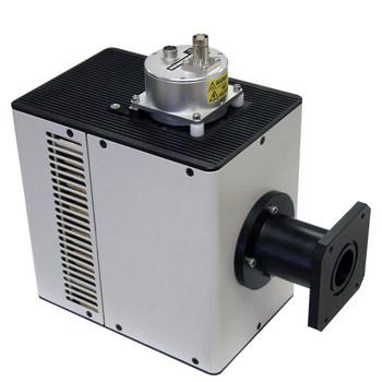
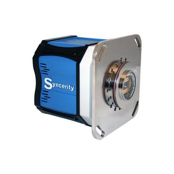
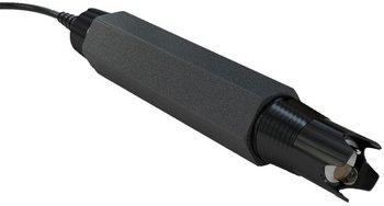
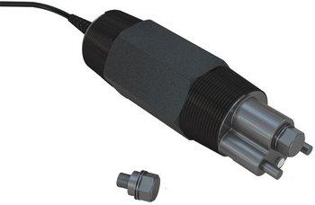
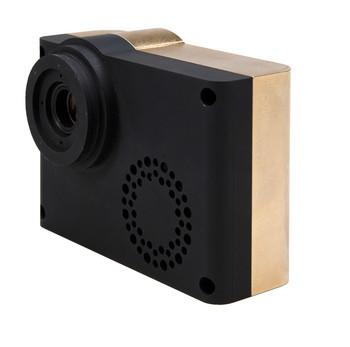
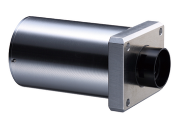
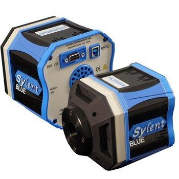
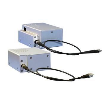
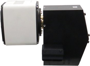
Photoluminescence Microspectrometer
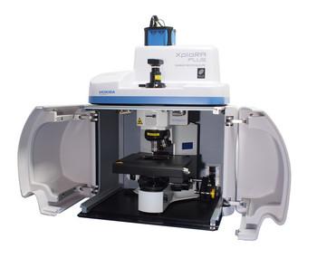
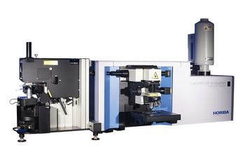
MicroRaman Spectrometer - Confocal Raman Microscope
Raman Spectroscope - Automated Imaging Microscope
Confocal Raman & High-Resolution Spectrometer
Flexible Raman System
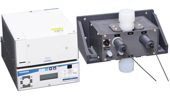
TCSPC/MCS Fluorescence Lifetime System
Steady State and Lifetime Benchtop Spectrofluorometer
TCSPC Lifetime Fluorometer
Blood Slide Stainer
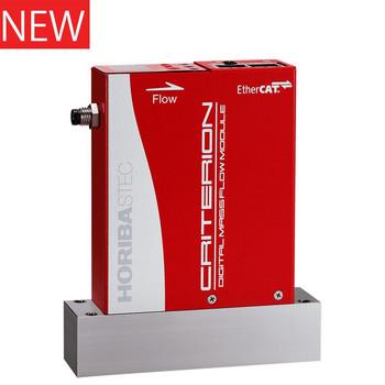
Micro Flow Pressure Insensitive Mass Flow Module
BET Surface Area Analyzers
Ultrasensitive molecular detection
DeltaRAM-X based millisecond QuantaMaster spectrofluorometer
For Single‐Walled Carbon Nanotube Excitation‐Emission Map Simulation and Analysis
Blood Smearing Device
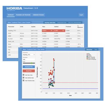
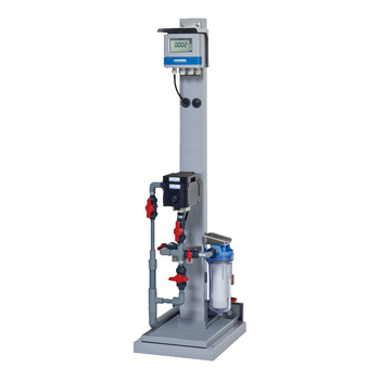
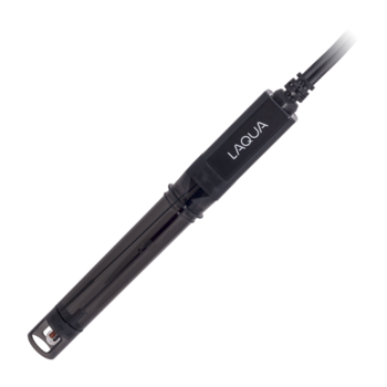
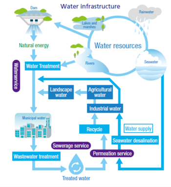
Modular Water Supply Quality Monitor
SPAD array imaging camera for dynamic FLIM studies at real time video rates
Blood Slide Stainer
Electric Vehicle Charge Monitor
Broadband Xe Light Source
Tube Sorter
Hemostasis Analyzer
Wafer Back Side Cooling System
Automatic Critical Flow Orifice
Hemostasis Analyzer
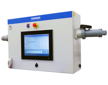
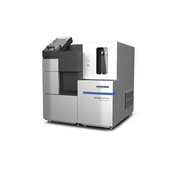
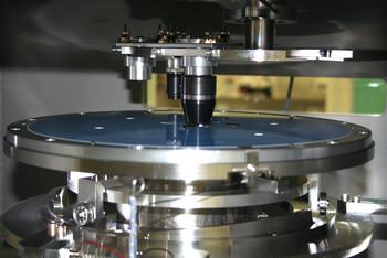
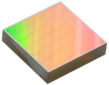
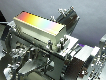
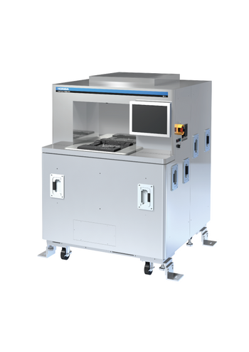
Photoluminescence and Raman Wafer Imaging
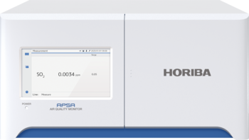
Air Quality Monitor
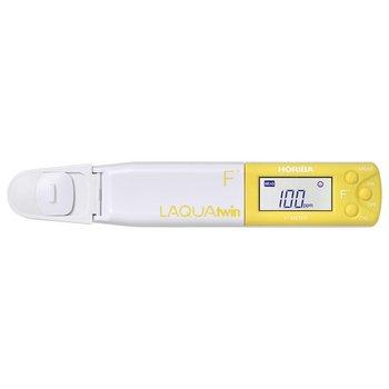
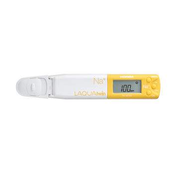
Pocket Potassium Meter
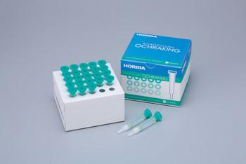
Hemostasis Reagents
Hydrogen Gas Analyzer
Scanning Probe Microscope with Chemical Signature
For Instant Water Quality Reports
TCSPC Pulsed Sources
Digital Cell Morphology System
AFLATOXINS / STERIGMATOCYSTIN Immunoaffinity column for Chemical pre-treatment
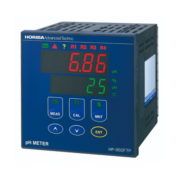
Pocket pH Meter
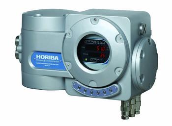
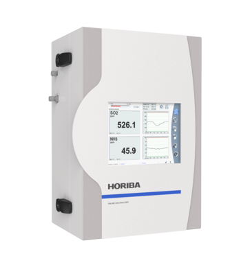
OEM gas (NO) analyzer
Hemostasis Reagents
Steady State Software
Simultaneous Multi-Laser Nanoparticle Tracking Analysis (NTA)
Digital Cell Morphology System
Ochratoxin analysis Immunoaffinity column for pre-treatment
Clinical Chemistry Analyzer
Collaborative Correlative Microscopy
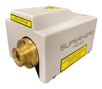
Forensic Light Source
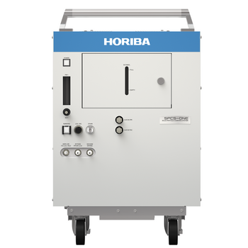
Solid Particle Counting System
Hemostasis Reagents
Software-controlled for automated temperature dependent fluorescence
Spectral Identification Assistant within Raman Spectra Database
Reticle / Mask Particle Detection System
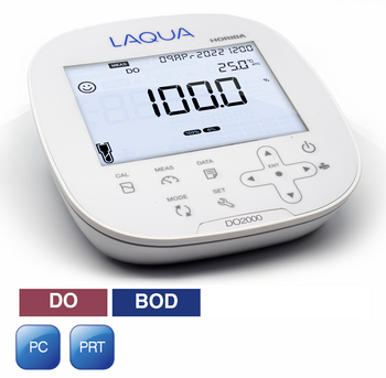
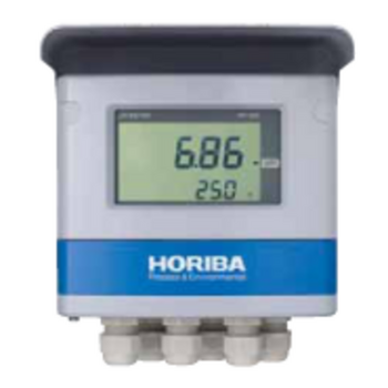
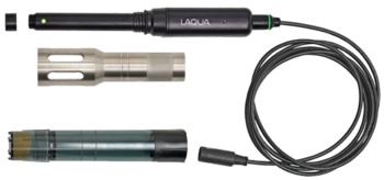
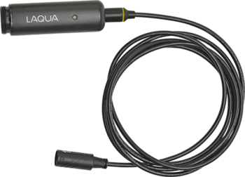
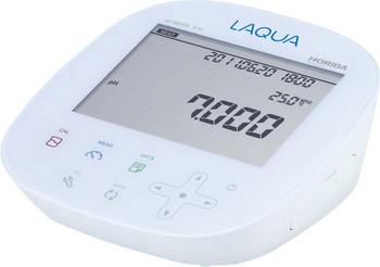
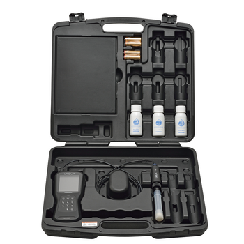
Benchtop pH/ORP/Ion/DO/BOD/Temperature Meter
Raman accessory for pharmaceuticals
Automated Organic Analysis & Early Warning Sentinel
Digital Cell Morphology System
Immunoaffinity column to clean up aflatoxins
Camera Endpoint Monitor based on Real Time Laser Interferometry
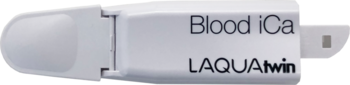
Bovine Calcium Meters
Real-time and Direct Correlative Nanoscopy
Greater Versatility and User Functionality
X-ray Analytical Microscope
with a Super Large Chamber
Oxygen/Nitrogen/Hydrogen Analyzer
(Flagship High-Accuracy Model)
Total Siloxane Analyzer
Hemostasis Reagents
Pocket Water Quality Meters
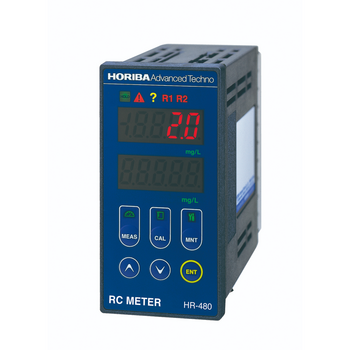
Residual Chlorine Concentration Monitor
Rapid Microorganism Detection System
Panel mount type water quality measuring instruments
Automated Raman D-to-G peak intensity ratio analysis for carbon materials
Test Automation Software for Battery Testing
Hematology and ESR Analyzer
Affordable high performance ICP-OES
Decay Analysis Software
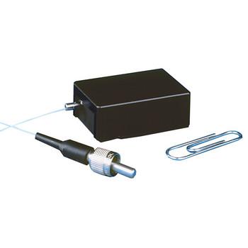
Fiber probes: High Efficiency Raman sensors
Global Hematology Solution
X-ray Analytical Microscope (Micro-XRF)
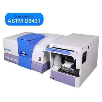
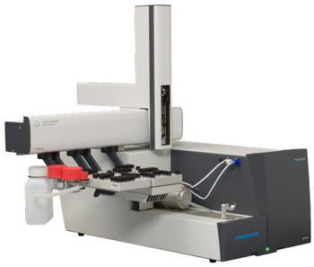
Aqualog A-TEEM Autosampler Accessory
Digital Cell Morphology Systems
OEM gratings design and production capabilities
Endpoint / Chamber Health Monitor based on Optical Emission Spectroscopy and MWL Interferometry
Process Laser Gas Analyzer
Centrifugal Nanoparticle Analyzer
Portable Automated Measuring System
Reticle / Mask Particle Detection System
Oxygen/Nitrogen Analyzer (Entry Model)
OEM gas (CO/HC) analyzer
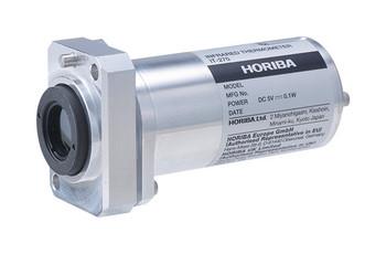
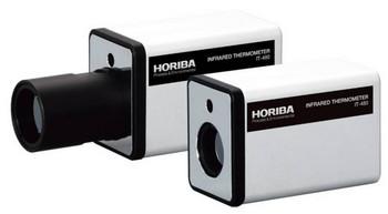
High-Accuracy Infrared Thermometer [Built-in type]
Hematology Analyzer
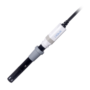
Benchtop DO/BOD/Temperature Meter
Gel-filled Self-Cleaning pH Electrode
Automated Analysis of Multilayers Materials
Hemostasis Reagents
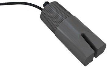
Nitrate Ion Sensor Cartridge
Pocket Water Quality Meters
Fluorescence Lifetime Imaging Platform
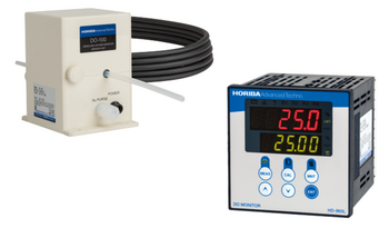
Dissolved Oxygen Concentration Monitor Series for Semiconductor Manufacturing
Standard type
Raman Calibration Objective
SPRi software suite for simple use and easy data analysis.
Raman Spectrometers
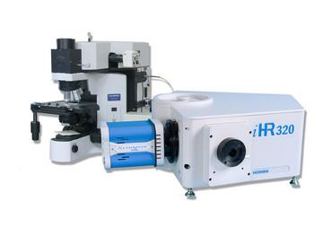
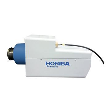
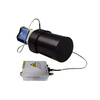
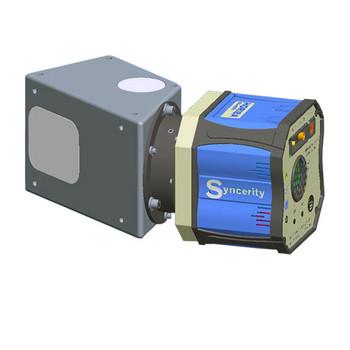
Raman Photoluminescence & Cathodoluminescence
Reflective Ultra Violet Imaging System
Handy Gloss Checker - New
Silica analyzer
High Spectral Rate and High Dynamic Range Miniature Spectrometers
EMCCD Scientific Camera
Oil concentration meter
Hematology Analyzer
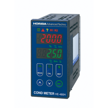
Conductivity Cell for Ultra Pure Water Measurement
Plastic body Non-refillable ORP electrode
Correlate Multiple Modalities with Ease
Next Generation Total Nitrogen and Total Sulfur Analyzer
Test Automation Software for Electrified Vehicle Testing
Miniature 18-Bit Spectrometer
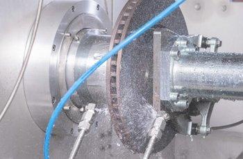
Brake Dynamometer for Brake Emissions Testing
Multichannel Spectrometer and Hyperspectral Line Imager
Hemostasis Analyzer
HORIBA’s latest development in TCSPC detector technology
Laser Spectroscopic Motor Exhaust Gas Analyzer
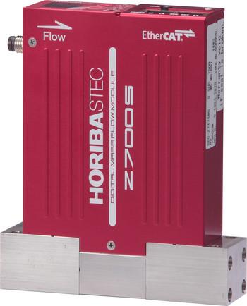
Best Performance Pressure Insensitive Mass Flow Module
Nitrogen Oxides Monitor
Large choice of PMTs, solid state, photoelectric detectors for custom spectroscopy solutions
Accreditation Support
On-site, intrinsically safe explosion-proof ORP meter
Dual Mode Analog/Photon Counting PMT
Accreditation Support
Hemostasis Analyzer
Ultra Fast TCSPC Lifetime Fluorometer
High-Accuracy Infrared Thermometers [Stationary type]
Panel-mount type dissolved oxygen meter (DO meter)
AFM-Raman for physical and chemical imaging
Pulsed-RF Glow Discharge Optical Emission Spectrometer
Raman Accessory for Imaging
Convert map data into chemical images
OEM gratings design and production capabilities
High Speed & Precision Pressure Insensitive Mass Flow Module
Industrial pH meter
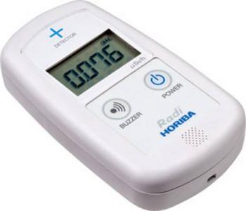
Environmental Radiation Monitor "Radi"
Deep Cooled Vacuum Ultra Violet Scientific Cameras
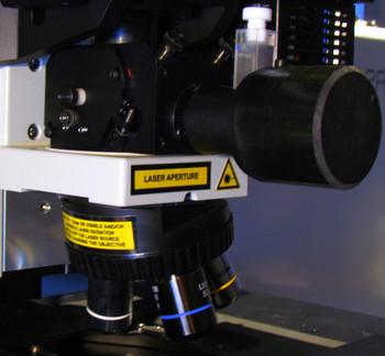
Connect any of our steady state and hybrid fluorometers to virtually any upright or inverted microscope!
High resolution, high sensitivity and high stability ICP-OES
LED Phosphorescence Light Sources
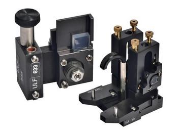
Laser Trapping Solution - Raman Accessory for Life Science
Forensic Light Source
Hematology Analyzer
Accreditation Support
Compact Deuterium, Tungsten Halogen or Glow Bar Light Source
X-ray Fluorescence Sulfur-in-Oil Analyzers
ORP Sensor Cartridge for WQ-300 series
Hydrogen Gas Analyzer
Reduce Vehicle Development Complexity
High Voltage Emulation
Hyperspectral Imaging Spectrometer
Run tests reliably and efficiently with automation
Field-installation type intrinsically safe explosion-proof pH meter
Gloss Checker
Hematology Analyzer
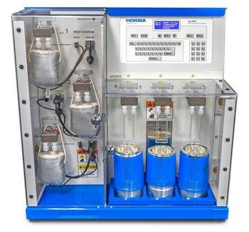
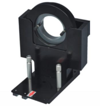
PLQY Integrating Sphere
Double-junciton type
For your specific application
Accessories for samples with various shapes, sizes and properties
Raman Accessory for Imaging
Data analysis for complex data sets
X-ray Fluorescence Sulfur-in-Oil Analyzer
OEM gratings design and production capabilities
Highest SNR PDA Miniature Spectrometer
Fiber Optic Type Chemical Solution Concentration Monitor
On-vehicle Ultrasonic Fuel Flow Meter
Wide Range Pressure Insensitive Mass Flow Module
High-Accuracy Infrared Thermometers [Handheld type]
ICP Software
Single photons detection with picosecond accuracy
Easy to deposit, easy to recover, easy to clean.
Hematology Analyzer
Hemostasis Analyzer
AFM-Raman for Physical and Chemical imaging
X-ray Fluorescence Sulfur/Chlorine-in-oil Analyzer
Miniature Multi Communication UV-NIR Spectrometer
Flat Carbon Sensor Conductivity Meter
Ultra-thin Mass Flow Module
Collect a wide range of data sources
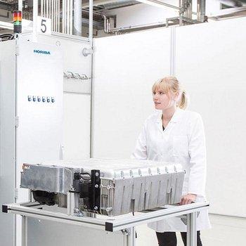
Solutions for Battery Development, Testing and Validation
End-of-Line Battery Testing Systems
Saltwater, Wet and Fog Testing for Brake Dynamometers
Hydrogen Fuel Flow Meter
Chassis Dynamometer
Field-installation type color meter
Oil concentration meter
Deep Cooled UV/Vis/NIR
Direct contact spotting
Quantum and Image
Tunable Broadband Light Sources
Précis Certified Standard
Customize your instrument
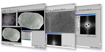
Automated Fingerprint and Palmprint Identification - AFIS & APIS Systems
OEM gratings design and production capabilities
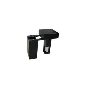
Versatile AFM Optical Coupling
High-Accuracy Infrared Thermometer [Built-in type]
Slide Preparation System
Raman Accessory for Calibration
Intuitive Auto-Soft Interface for the Auto SE and Smart SE
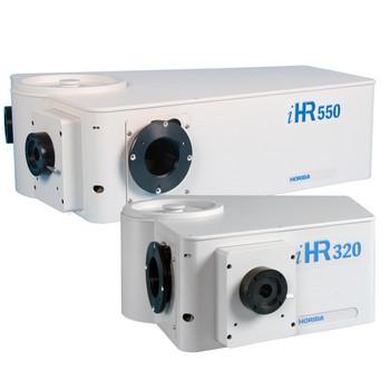
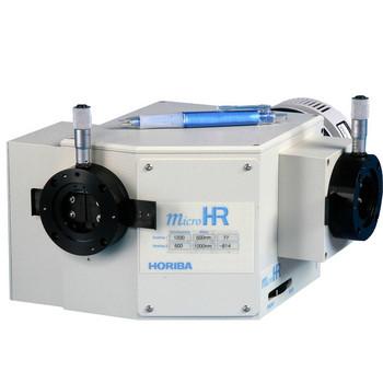
Imaging Scanning Monochromator
Optical Fiber Type Hot Phosphoric Acid Concentration Monitor
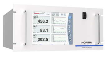
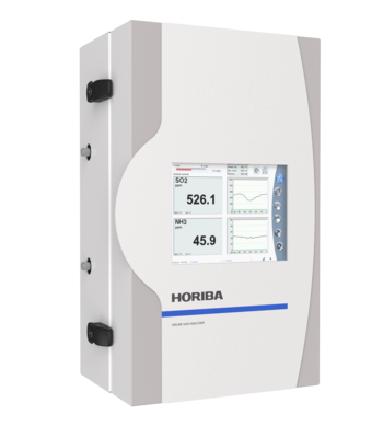
Online Gas Analyser
Clinical Chemistry Analyzer
Rapid Raman Plate Reader – Multiwell Fast Raman screening
Online Gas Analyser
Clinical Chemistry Analyzer
Online Gas Analyser
Road-to-Rig Chassis Dyno Replication
Clinical Chemistry Analyzer
Create Simulation Models from Real Hardware
Online Gas Analyser
Hydrocarbon Monitor
Clinical Chemistry Analyzer
Sulfur Dioxide Monitor
Online Gas Analyser
Facility & Asset Management Software
Ozone Monitor
Online Gas Analyser
Field-installation Type Fluoride Ion Concentration Meter
Hemostasis Analyzer
Amplifier-Discriminator
Complete your ICP-OES Spectrometer for your specific needs
A Platform for HORIBA Scientific Ellipsometers
High Sensitivity Imaging Spectrograph
Versatile Hyperspectral Cathodoluminescence
OEM gratings design and production capabilities
Fuel Flow Measurement Systems
New concept Pressure Insensitive Mass Flow Module
Optimized Analytical Workflow
Software Solutions
Carbon Monoxide Monitor
Affordable Benchtop Raman Spectrometer
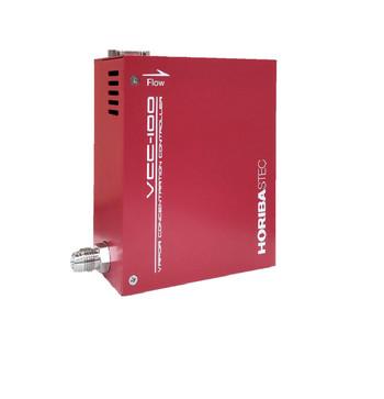
Vapor Concentration Controller
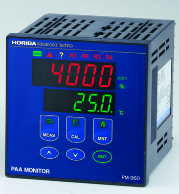
Peracetic acid concentration monitor
Panel-mount type galvanic residual chlorine meter
Hemostasis Analyzer
Accreditation Support
MINI-CCT+ Mini Raman Spectrometer
Compact Hyperspectral Cathodoluminescence
Automatic Driving System
Non-Contact Chemical Concentration Monitor
Thermal Flow Splitter
A Simple, Fast, “Column Free” Molecular Fingerprinting Technology
Mono & Multi-Channel Water Controller
Multi-Channel Water Controller
Online Analyser for Drinking Water
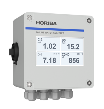
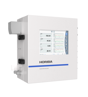
Online Water analyzer
Deep Cooled High Speed Scientific CMOS Camera
Online Water Analyser
Cost-effective, High-performance Mini Spectrometer
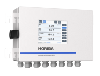
Online Water Analyzer
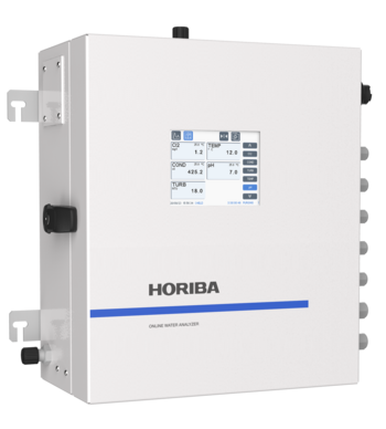
Online Water Analyser
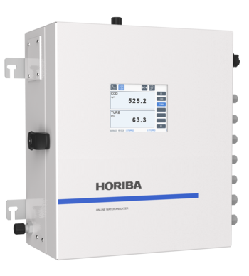
Online Water Analyser
Oil concentration meter
Hemostasis Analyzer
Automated Conveyor
Hematology Analyzer
Hematology Analyzer
Hydrogen Analyzer
Deep Cooled NIR Scientific Cameras
Manual label-free molecular interaction analysis machine Flexible Research Platform
Tunable 75W Xe Light Source
Raman Accessory for fast imaging
E-Motor Testing
OEM gratings design and production capabilities
Panel-mount type polarographic residual chlorine meter
Hemostasis Analyzer
Hematology Analyzer
Highly sensitive silica monitor for ultra-pure water management in semiconductor/FPD processes
Hematology Analyzer
Hematology Analyzer
AFM and inverted light microscopy
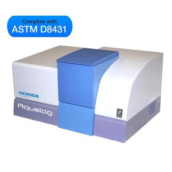
The Gold Standard for Water CDOM Research
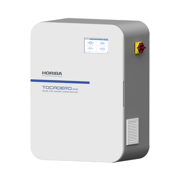
Automatic Total Organic Carbon Analyzer (On-line TOC analyzer)
Compact Spectrometer for OCT
Ammonia Monitor
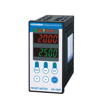
Field-installation type electric resistivity meter (resistivity meter)
Middleware and expert validation station
Powerful and Cost Effective Spectroscopic Ellipsometer
Software for Laboratory Management
Space qualified and TRL9
Hematology Analyzer
The AFM optical platform
Microwave Digestion Vessels
Portable Gas Analyzer
Panel-mount type 2-channel electric resistivity meter (resistivity meter)
Large Flow Liquid Source Vaporization Control System
Carbon/Sulfur Analyzer (Tubular Electric Resistance Heating Furnace Model)
Process Analyzer System
Clinical Chemistry Analyzer
Hematology Analyzer
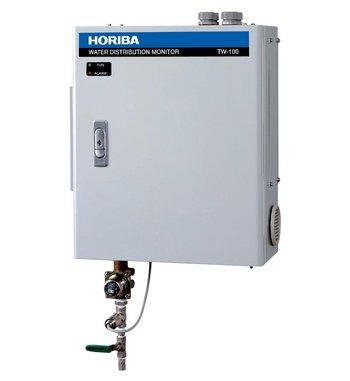
Water distribution monitor
Field-installation type electric conductivity meter (conductivity meter)
Hematology Analyzer
Six position electric Fluxer
Cathodoluminescence Solutions for Electron Microscopy
Spectroscopic Ellipsometer for Simple Thin Film Measurement
Modular Research Fluorometer for Lifetime and Steady State Measurements
Ultra Compact and Broad Range Spectrometer
Multi-Component Gas Analyzer
Clinical Chemistry Analyzer
Phosphoric Acid Monitor
Pocket Water Quality Meters
Continuous Emission Monitoring System
Advanced stand-alone AFM
Ambient Hydrogen Sulfide (H2S) Monitor
Ambient Sulfur Dioxide Monitor
Function Control Unit by Remote Control
Function Control Unit with Mass Flow Controllers
Tunable Laser Gas Analyzer
pH meter with automatic calibration function
Field-installation type ORP meter
Panel-mount type resistivity meter (resistivity meter)
Hematology Analyzer
Carbon/Sulfur Analyzer
(Flagship High-Accuracy Model)
Spectroscopic Ellipsometer from FUV to NIR: 190 to 2100 nm
High Resolution Monochromators
Holographic Lamellar Gratings
Altitude Simulator
Automatic Acquisition of Raman Spectra at Multiple Positions
Automatic Span Gasgenerator Unit
Automatic Span Gas Unit for Parallel calibration
Automatic Span Gas Unit for Serial calibration
Automatic Span Gas Unit Transferstandard
Automatic Span Gas Generator Unit for Quality control at field test
Explosion-proof Gas Analyzer
Clinical Chemistry Analyzer
In-line Sensor & Auto Range Switching Concentration Monitor
Software Control and Data Acquisition
Reliable, efficient TERS probes for AFM-Raman imaging
High Throughput Chemical Screening Experiments
Altitude Simulation
Water distribution monitor
Ambient Carbon Dioxide Monitor
Field-installation type ammonia nitrogen meter
Hematology Analyzer
Fiber Optic Type Chemical Concentration Monitor
Pocket Water Quality Meters
Choose from a large assortment of optical components for your custom spectroscopy solutions
for UV Raman spectroscopists
Compact High Resolution CMOS or CCD Spectrometer
High-grade type Gas Monitor for Chamber Cleaning End Point Monitoring
Automated Particle Measurement, Identification and Classification using Raman Analysis
Powertrain Testing for Front, Rear and All Wheel Drive
Washwater Monitoring System
Ultra-compact Scientific Uncooled CMOS Camera
Panel-mount type conductivity meter
Carbon/Sulfur Analyzer (Entry Model)
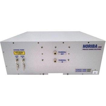
High efficiency dedicated process Raman spectrometer for rugged and robust Raman monitoring.
Pulse compression gratings using holographic techniques
UV-VIS-NIR EMCCDs Camera
Laser scanning oil film detector
Pocket Water Quality Meters
Acquire the Topography of the Analyzed Sample & sharp, In-Focus Raman Images
Fiber coupled microscope
Swing mill with sound-proof enclosure that accommodates sample sizes ranging from 2 - 100 grams
Deep Cooled UV/Vis/NIR and VUV Scientific Cameras
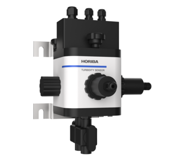
Field-installation type turbidity meter
Panel-mount type 2-channel conductivity meter (conductivity meter)
Multispectra, Multifiber, Multichannel Imaging spectrometer with 8-16-32 Simultaneous UV-NIR Spectra
UV-VIS-NIR Spectrometer
Plasma Emission Controller
Navigate your sharp image in real-time
Spectroscopy and imaging software
Field-installation type turbidity meter
Stack Gas Analyzer
Automatic total nitrogen/phosphorus monitor
Pressure Insensitive Mass Flow Module
Low Concentration Monitor- Sulfuric Acid/Hydrogen Peroxide
Engine Test Stand System
Data Management and Reporting Software
Large cryogenic mill that accommodates sample sizes ranging from 0.1 - 100 grams.
Stack Gas Analyzer
Test Automation Software for Engine Testing
Panel-mount type conductivity meter (conductivity meter)
Stack Gas Analysis System
Multichannel Grating Spectrometer
Small Volume Circulation System
On-board NH3/N2O Measurement System for real-world driving
Test Automation Software for Heavy-Duty Engine Emission Testing
Automatic COD monitor
Mixed Injection System Liquid Vaporizer
Lets you navigate easily through your image
Test Automation Software for Powertrain Testing
Field-installation type turbidity/SS meter
8 hot blocks controlled by one wireless commander!
Hyperspectral Imaging Spectrometer Applications
Engine Torque Pulse Simulation
Organic pollutant monitor
Test Gas Generation Systems
Pocket Water Quality Meters
Mid-Focal Length Imaging Spectrometers
Field-installation type turbidity meter
Mixed Gas Generators MU Series
On-board SPN10 measurement for real-world
Flexible Turn Key Solution for Test Beds
Multi-parameter water quality checker
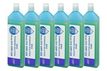
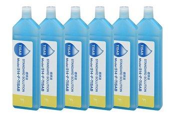
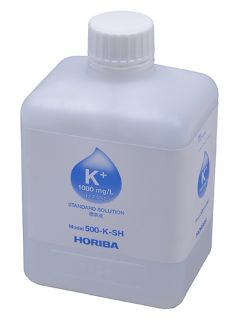
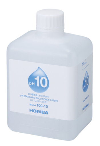
1.41 mS/cm Conductivity Standard Solution
Most Compact Vacuum UV Back-Illuminated CCD Spectrometer (VUV-FUV)
FTIR Exhaust Gas Analyzer Dilute Measurement Type
Test Automation Software for Brake Testing
Field-installation type electrical conductivity meter (conductivity meter)
Panel-mount type conductivity meter (conductivity meter)
Pocket Water Quality Meters
12.9 mS/cm Conductivity Standard Solution
Hydraulic Dynamometers
Ambient Carbon Monoxide Monitor
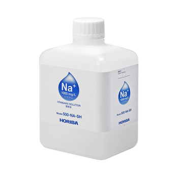
0.5% NaCl Standard Solution
Short Focal Length Imaging Spectrometers
Nanoparticle Analyzer
Dual Pitot Tube Exhaust Flow Meter
卓上型pHメータ
Air Pollution Monitor
Eddy Current Dynamometers
Field-installation Type Fluoride Ion Concentration Meter
Panel-mount type ORP meter
5.0% NaCl Standard Solution
Small cryogenic mill that accommodates sample sizes ranging from 0.1 - 4 grams.
Ultra Fast Raman Imaging for detailed Raman maps
X, Y, Θ Position Calibration Plate For Machine Vision and Microscopy
Test Automation Software for Emission Testing
Air Pollution Multigas Calibrator
Pocket Water Quality Meters
X, Y, Θ Absolute Position Encoder
Turns Raman Imaging from Hours to Minutes
Field-installation type pH meter
Panel-mount type pH meter with 4-point alarm time sharing proportional control
Vapor Concentration Monitor
Small high-energy ball mill that accommodates sample sizes ranging from 0.2 - 1.5 grams.
DUAL & QUAD CCD Mini-Spectrometer
Test Automation Software for Durability Testing
Field-installation type electric resistivity meter (resistivity meter)
Panel-mount type pH meter with industrial time sharing proportional control
High-energy ball mill that accommodates sample sizes ranging from 0.2 - 10 grams.
Pocket Water Quality Meters
Ambient Air Quality Monitoring System
Ambient Dust Monitor
Field-installation type electric conductivity meter
Micro Volume pH Monitor
Hot Blocks for Acid Digestion
Interface level meter
Panel-mount type pulse proportion control pH meter
Pocket Water Quality Meters
Mini Raman Spectrometer
Pitot Tube Exhaust Flow Meter
Field-installation type dissolved oxygen meter (DO meter)
Large cryogenic mill that accommodates sample sizes ranging from 0.1 - 100 grams.
Superior and Intelligent Controller Platform
H2O2 Monitor
Pocket Water Quality Meters
Protection Case for Testing Heavy-Duty and Non-Road Mobile Machinery
Multi-Purpose Brake Dynamometers
Field-installation type ORP meter
Panel-mount type pH meter
Close Vessel Microwave Digestion System
OEM CCD Camera
Motor Exhaust Gas Analyzer
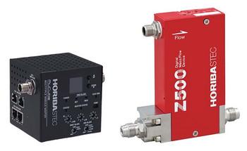
Digital Mass Flow Controller
Field-installation type polarographic residual chlorine meter
Pocket Water Quality Meters
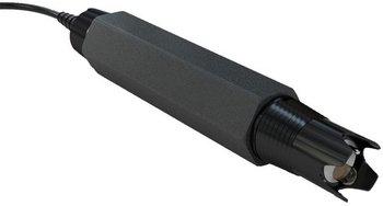
Laser-induced Breakdown Spectroscopy (LIBS)
Close Vessel Microwave Digestion System
Organic pollutant monitor
Laser Scattering Particle Size Distribution Analyzer
Brake Test Systems
Field-installation type dissolved oxygen meter (DO meter)
Pocket Water Quality Meters
Automated Hot Block
Particulate Filter Management System
Digital Automatic Pressure Regulator
Resistivity Meter for Semiconductor Cleaning Processes
OEM Miniature Raman Systems and Components
Field-installation type MLSS meter
Miniature High Throughput Spectrometer
Automated Workstation
Sampling System
Micro Dilution Tunnel
Brake Test Systems
Industrial pH meter
Field-installation type optical dissolved oxygen meter (DO meter)
Steady-State Engine Test Stand System
Stand-alone Type Chemical Concentration Monitor
On-board Emissions Measurement System
Field-installation type pH meter
PTFE Filter/TFH membrane
Unique fluorescence removal tool
High-throughput tissue homogenizer with an adjustable clamp.
Low Inertia Series - AC Dynamometer
Field-installation type residual chlorine meter
Instant Raman Analysis
Continuous Particulate Monitor with X-ray Fluorescence
OEM Raman Filters
Multivariate Analysis App for all Raman Maps
Transient Engine Test Stand System
Handheld Water Quality Meters
FTIR Motor Exhaust Gas Analyzer
On-line TOC analyzer
Automated Tissue Homogenizer
On-board Emissions Measurement System
Dynamic Engine Test Stand System
High Temperature Digital Mass Flow Controller
Low Concentration Type HF/HCl/NH3 Concentration Monitor
Raman Spectral Searching
On-board Emissions Measurement System
Hydrocarbon Monitor / THC Analyser
Pressure Insensitive Mass Flow Controller
Swing mill that accommodates sample sizes ranging from 2 - 100 grams.
Automated Silicon Stress Analysis
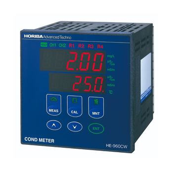
Insertion sensor type for wide-range conductivity meter HE-960HI
Reticle/Mask Particle Remover
Automated DLC Coating Analysis
Laser Spectroscopic Motor Exhaust Gas Analyzer
AC Dynamometer
Hybrid Chemical and Video Image Display
Ambient Dust Monitor
Wide range TMAH Concentration Monitor
Total Halogen and Sulfur Analyzer
Ultrasonic Exhaust Flow Meter
High Torque Series - AC Dynamometer
Optical Emission Spectroscopy Etching End-point Monitor
3D confocal volume control and display
Total Nitrogen and Sulfur Analyzer
Ambient Ozone Monitor
HF / HCl Concentration Monitor
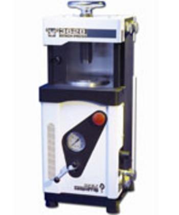
Full-size 12-ton (10.9 metric ton) Carver hydraulic laboratory pellet press.
Constant Volume Sampler
Ambient NOx Monitor
Carbon Sensor Conductivity Meter (High concentration type)
Bench top 12-ton (10.9 metric ton) Carver hydraulic laboratory pellet press.
Motor Exhaust Gas Analyzer
Heavy Duty Series - AC Dynamometer
Ambient Sulfur Dioxide Monitor
Carbon Sensor Conductivity Meter (Low concentration type)
Water Quality Monitoring System
25-ton (22.7 metric ton) air-actuated laboratory pellet press.
Field-installation type water quality measuring instruments
High Performance Series - AC Dynamometer
Ambient Ammonia Monitor
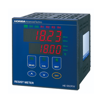
2-Channel Resistivity Meter
OEM miniature spectrograph
Ambient Hydrogen Sulfide Monitor
Carbon Sensor Resistivity Meter
35-ton (31.8 metric ton) hydraulic laboratory pellet press.
Emphasize Raman and Optical Images
Trace Gas Monitor
Datalogger IO-Expander
Create templates for fast data reports
Ozone Transferstandard
Conversion Adapters
High throughput data processing
Zero Gas Generator
Zero Gas Generator
Fast and easy Raman acquisition
Full-size 25-ton (22.7 metric ton) Carver hydraulic laboratory pellet press.
Setting Units
Recall settings, and automate processes
Citric Acid Monitor
Display Unit
Customize with VBS
Dedicated power sources
Cooled fluorescence imaging cameras
Digital Controller
Carbon Sensor Conductivity Meter
Control Unit
Solid Particle Counting System
Monitor Unit
Single Channel Controller of Hot Block
Dynamic Altitude Simulation
Regulatory compliance and data integrity
Only available for volume OEM purchase, minimum order quantity 50 units.
Handheld Water Quality Meters
Particle Disperser
Test Unit for Fuel Measurement Systems
High Precision, High Stability Chemical Concentration Monitor
Password protected user access control
Handheld Water Quality Meters
Model Size System
Air-to-fuel Ratio Analyzer
Handheld pH/ORP/Dissolved Oxygen/Temperature Meter
Full Size System
HF (Hydrofluoric Acid) DO (Dissolved Oxygen) Monitor / Pure Water DO (Dissolved Oxygen) Monitor
Alignment and calibration tools
Handheld pH/ORP/Dissolved Oxygen/Temperature Meter
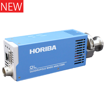
Quadrupole Mass Analyzer
High Speed Series - AC Dynamometer
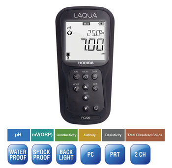
Handheld pH/ORP/Conductivity/Resistivity/Total Dissolved Solids/Salinity/Temperature Meter
Wafer Back Side Cooling System
LabSpec 6 is a validated software
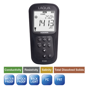
Handheld pH/ORP/Conductivity/Resistivity/Total Dissolved Solids/Salinity/Temperature Meter
Handheld Conductivity/Resistivity/Salinity/Total Dissolved Solids/Temperature Meter
Benchtop Conductivity/Resistivity/Total Dissolved Solids/Salinity/Temperature Meter
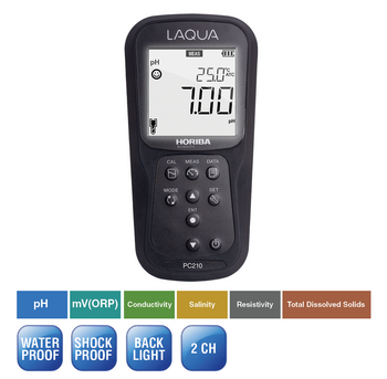
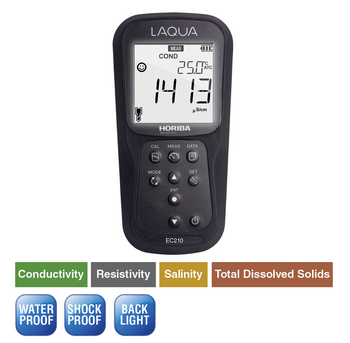
Handheld Conductivity/Resistivity/Salinity/Total Dissolved Solids/Temperature Meter
Exhaust Pressure Controller
Benchtop pH/ORP/Ion/Conductivity/Resistivity/Total Dissolved Solids/Salinity/Temperature Meter
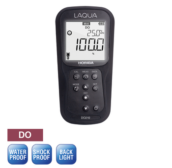
Handheld Dissolved Oxygen/Temperature Meter
Dissolved Ozone Monitor
Digital Liquid Mass Flow Meters / Controllers
Handheld Dissolved Oxygen/Temperature Meter
Compact Baking System
Benchtop pH/ORP/Ion/Temperature Meter
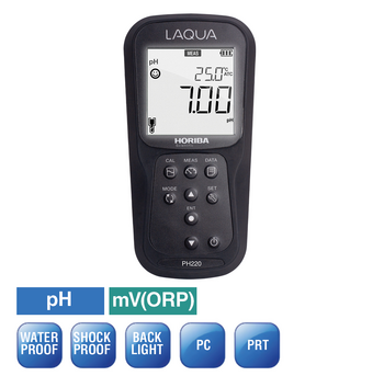
Handheld pH/ORP/Temperature Meter
High Precision TMAH Concentration Monitor
Liquid Auto Refill System
Handheld pH/ORP/Temperature Meter
Mass Flow Checker
Benchtop pH/ORP/Ion/Temperature Meter
KOH Monitor
Mixed Injection System Liquid Vaporizers
Piezo Actuator Valve
Mass Flow Controller
Direct Liquid Injection System
Multi Range/Multi Gas Digital Mass Flow Controller
Standard type
Heated Type NOx Analyzer
For measurement of low-conductivity water and non-aqueous solvents.
Heated Type THC Analyzer
Motor Exhaust Gas Sulfur Analyzer
Automotive Emission Analyzer
FTIR Exhaust Gas Analyzer Direct Measurement Type
X-Ray Fluorescence Analyzer
X-Ray Fluorescence Analyzer
Energy Dispersive X-ray Fluorescence Analyzer
X-ray Fluorescence Sulfur-in-Oil Analyzer
X-ray Fluorescence Sulfur-in-Oil Analyzer
Do you have any questions or requests? Use this form to contact our specialists.


 6560S-10C")

")
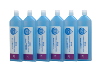
 Y021H")


![APNA-370/CU-2 [High Sensitivity Model]](http://static.horiba.com/fileadmin/Horiba/_processed_/7/4/csm_5_APNA-370_CU-2__NH3___high_sensitivity__ppb__901fa929c1.png)


![APSA-370/CU-1 [High Sensitivity Model]](http://static.horiba.com/fileadmin/Horiba/_processed_/e/2/csm_3_APSA-370_CU-1__H2S___high_sensitivity__ppb__0be5546310.png)
![APSA-370 [High Sensitivity Model]](http://static.horiba.com/fileadmin/Horiba/_processed_/6/2/csm_APSA-370_Ambient_Sulfur_Dioxide_Monitor_Products_image_B_0aa51056b9.png)


")


 Y021L")
")


 6561S-10C")


 Y071H")

")


 Y071L")

")


 5002S-10C")


")
")


")


")


")


 6583S-10C")


")


")


")


")
")
")


")


")


")


,HE-960LC")


")


")


")


")


")


")


")


")


")
")


")


")


")
")


")

")


