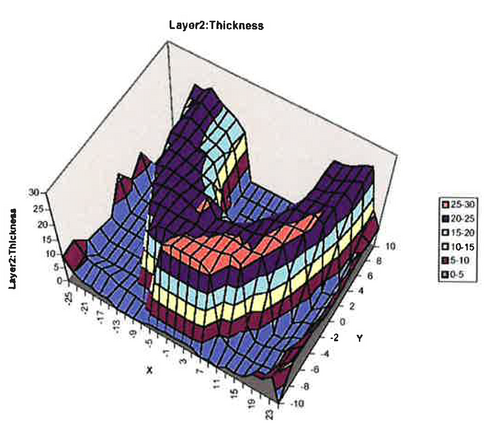
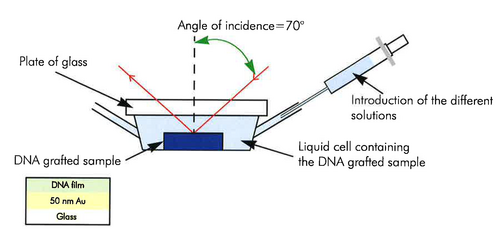
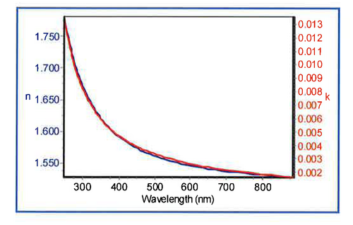
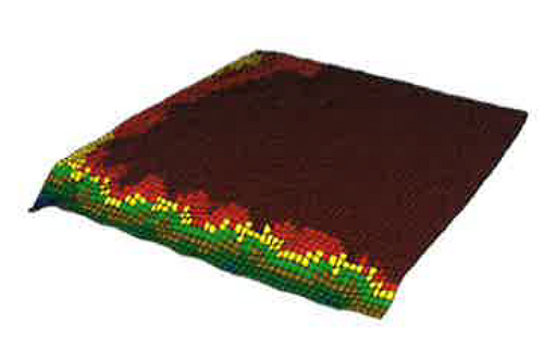
Characterization of DNA sensor pads using UVISEL Spectroscopic phase modulated Ellipsometer

Spectroscopic Ellipsometer from FUV to NIR: 190 to 2100 nm
UVISEL Plus ellipsometer 는 박막, 표면 및 물성 특성 측정/분석 특성화 장비 입니다.
각 구성이 모듈화 되어 있어 고성능 분석을 위한 최상의 조합을 자랑합니다.
UVISEL Plus는 보다 빠르고 정확하게 측정하도록 설계된 최신 기술을 적용시켰습니다. 최신 기술인 FastAcq 기술은 박막특성 측정/분석을 위해 설계된 double modulation 광학 기술을 기반으로 합니다.
새로운 전기적 신호, 데이터 처리 및 고속 분광기를 기반으로 하는 FastAcq 기술은 190 nm에서 2100 nm까지의 파장 영역의 측정을 고분해능으로 3분 이내에 측정할 수 있습니다.
UVISEL Plus 엘립소미터는 phase modulation (위상 변조_HORIBA 특허)기술을 기반으로 190 ~ 2100 nm의 스펙트럼 범위를 연속적으로 커버할 수 있는 강력한 광학 설계를 기반으로 합니다. 높은 정확도, 고해상도 측정 및 우수한 신호 대 잡음비 광학 시스템으로 고품질 데이터를 전체 스펙트럼 범위에 걸쳐 취득이 가능 합니다.
phase modulation technology(위상 변조 기술)는 기계적인 움직임 없이 고주파(50,000 Hz)위상 변조법으로 편광 변화를 측정하는 것이 특징입니다.
결과:
FUV(극자외선)와 NIR(근적외선)의 신호/잡음비가 우수
UVISEL Plus의 모듈식 설계를 통해 벤치탑 계측 툴로 사용하거나 디스플레이, 반도체 공정의 in-situ 에 사용하거나 롤투롤(roll to roll) 공정에 사용할 수 있습니다.
UVISEL Plus는 호리바가 제공하는 DeltaPsi2 소프트웨어 플랫폼(DeltaPsi2 software platform) 또는 모든 HORIBA 타원엘립소미터에 공통적으로 사용되는 Auto-Soft 인터페이스에 의해 제어됩니다.
DeltaPsi2는 일상적인 박막 분석/응용 프로그램과 고급 박막 응용 프로그램을 모두 다룰 수 있는 완벽한 측정 및 모델링 패키지를 제공하며, Auto-Soft 인터페이스는 직관적인 인터페이스를 통해 데이터 수집 및 분석을 효율적으로
진행할 수 있도록 도움을 줍니다.
UVISEL Plus와 FastAcq 기술은 재료 연구 및 가공, 평판 디스플레이, 마이크로 일렉트로닉스 및 광전지 분야에서 박막 두께 및 광학 상수 측정을 위한 가장 다재다능한 분광타원엘립소미터입니다.
UVISEL Plus는 재료 과학을 위한 Reference ellipsometer입니다.
Product benefits
Obtained information
UVISEL Specifications
Manual Configuration
Automatic Configuration
Integrated Goniometer
In situ configuration
Options
Performance


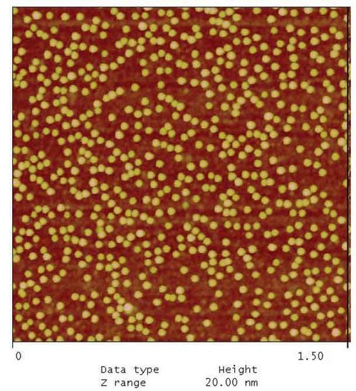
 and C70 (b) fullerenes.")


")


HORIBA제품의 자세한 정보를 원하시면, 아래의 양식에 내용을 입력을 부탁드립니다.
A Platform for HORIBA Ellipsometers

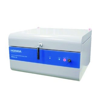
산소/질소/수소 분석기
산소/질소/수소 분석기
Glow Discharge Optical Emission Spectrometer

Raman Microscope

Powerful and Cost Effective Spectroscopic Ellipsometer

Spectroscopic Ellipsometer from FUV to NIR: 190 to 2100 nm
Raman Spectrometer - Confocal Raman Microscope

Spectroscopic Ellipsometer for Simple Thin Film Measurement

Camera Endpoint Monitor based on Real Time Laser Interferometry
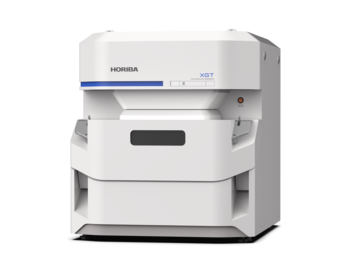
X선 형광 분석기
X선 형광 분석기

Powerful and Cost Effective Spectroscopic Ellipsometer

Spectroscopic Ellipsometer from FUV to NIR: 190 to 2100 nm
X선 분석 현미경(Micro-XRF)
X선 분석 현미경 초대형 챔버 모델

Spectroscopic Ellipsometer for Simple Thin Film Measurement
Powerful and Cost Effective Spectroscopic Ellipsometer
Spectroscopic Ellipsometer from FUV to NIR: 190 to 2100 nm

