

Size:
1.34
MB
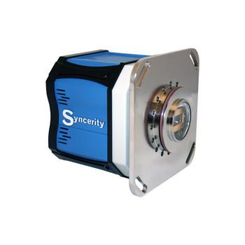
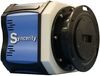
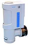
Syncerity OE Specification Sheet
Deep Cooled UV/Vis/NIR
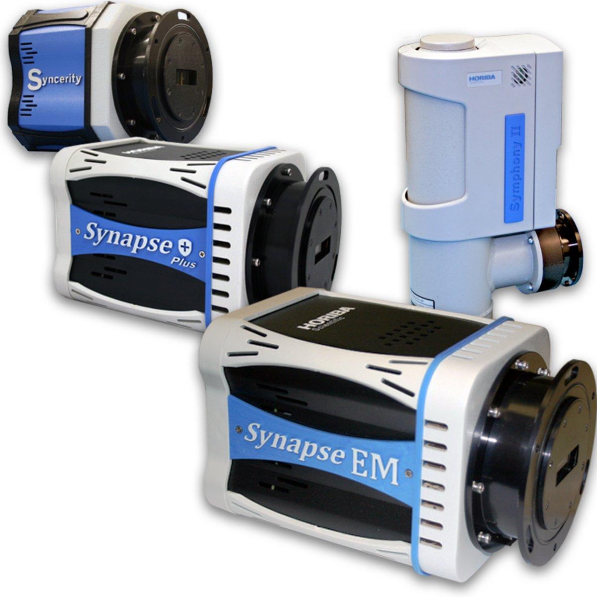
HORIBA Scientific offers a complete line of spectroscopic multi-channel detectors for scientific research. For spectral detection from UV to near-IR, two dimensional CCDs and indium gallium arsenide linear arrays offer a faster acquisition option over single point detectors with relatively high sensitivity. Coupled with HORIBA’s range of aberration corrected, flat field imaging spectrographs, custom spectroscopy packages can be assembled for a variety of applications.
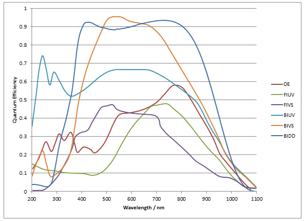
*OE- open electrode, FIUV- front illuminated UV enhanced, FIVS- front illuminated visible, BIUV- back illuminated UV enhanced, BIVS- back illuminated visible, BIDD- back illuminated deep depletion
| Cooling | Type* | Peak QE | Array Dimension | Pixel Size |
|---|---|---|---|---|---|
Syncerity | TE -60°C | 58% | 1024 x 256 | 26µm x 26µm | |
TE -50°C | 78% | 2048 x 70 | 14µm x 14µm | ||
SynapsePlus High Speed CCD | TE -80°C | 56% | 1024 x 256 | 26µm x 26µm | |
47% | 2048 x 512 | 13.5µm x 13.5µm | |||
48% | 2048 x 512 | 13.5µm x 13.5µm | |||
95% | 1024 x 256 | 26µm x 26µm | |||
75% | 1024 x 256 | 26µm x 26µm | |||
<90% | 1024 x 256 | 26µm x 26µm | |||
Synapse CCD | TE -75°C | ||||
56% | 512 x 512 | 24µm x 24µm | |||
95% | 512 x 512 | 24µm x 24µm | |||
75% | 512 x 512 | 24µm x 24µm | |||
Symphony II CCD | LN2-133°C | 58% | 1024 x 256 | 26µm x 26µm | |
56% | 1024 x 256 | 26µm x 26µm | |||
58% | 1024 x 256 | 26µm x 26µm | |||
95% | 1024 x 256 | 26µm x 26µm | |||
75% | 1024 x 256 | 26µm x 26µm | |||
95% | 1024 x 256 | 26µm x 26µm |
*OE- open electrode, FIUV- front illuminated UV enhanced, FIVS- front illuminated visible, BIUV- back illuminated UV enhanced, BIVS- back illuminated visible, BIDD- back illuminated deep depletion
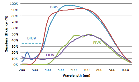
*FIUV- front illuminated UV enhanced, FIVS- front illuminated visible, BIUV- back illuminated UV enhanced, BIVS- back illuminated visible, BIDD- back illuminated deep depletion
Cooling | Type* | Peak QE | Array Dimension | Pixel Size | |
|---|---|---|---|---|---|
Synapse EMCCD | TE -60°C | 49% | 1600 x 200 | 16µm x 16µm | |
49% | 1600 x 200 | 16µm x 16µm | |||
95% | 1600 x 200 | 16µm x 16µm | |||
95% | 1600 x 200 | 16µm x 16µm | |||
92% | 1600 x 200 | 16µm x 16µm |
*OE- open electrode, FIUV- front illuminated UV enhanced, FIVS- front illuminated visible, BIUV- back illuminated UV enhanced, BIVS- back illuminated visible, BIDD- back illuminated deep depletion
Cooling | Wavelength | Array Dimension | Element Size | |
|---|---|---|---|---|
Synapse InGaAs | TE -60°C
| 800-1650 nm | 512 x 1 | 25µm x 500µm |
1050-2100 nm | 512 x 1 | 25µm x 250µm | ||
Symphony II InGaAs | LN2-103°C | 800-1600 nm | 512 x 1 | 25µm x 500µm |
1000-2050 nm | 512 x 1 | 25µm x 250µm |
Sie haben Fragen oder Wünsche? Nutzen Sie dieses Formular, um mit unseren Spezialisten in Kontakt zu treten.
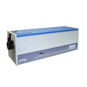
Long Focal Length Spectrometer
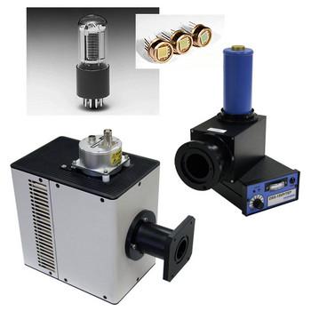
Dual Mode Analog/Photon Counting PMT
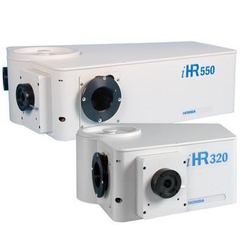
High Resolution Monochromators
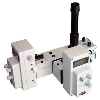
Double monochromator
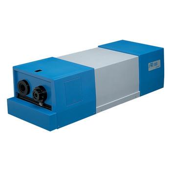
Mid-Focal Length Imaging Spectrometers
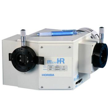
Short Focal Length Imaging Spectrometers
Ideal for Electrophysiology researchers to quantitate light intensity out of a microscope
Self contained PMT housing for quantitative spectroscopy and imaging low light measurements
Large choice of PMTs, solid state, photoelectric detectors for custom spectroscopy solutions
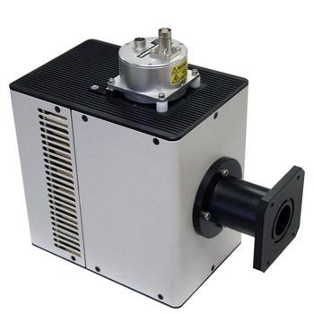
EMCCD Scientific Camera
Deep Cooled NIR Scientific Cameras
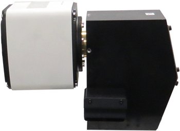
OEM CCD Camera
Deep Cooled Vacuum Ultra Violet Scientific Cameras