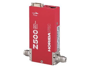
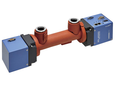
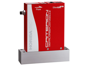
Mass Flow Module
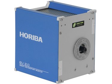
Deposition process is a key step in the semiconductor industry. HORIBA offers a wide range of products to optimize this process and to increase the yield
Atomic layer deposition (ALD) is a thin-film deposition technique based on the sequential use of a gas phase chemical process. ALD is considered a subclass of chemical vapour deposition. The majority of ALD reactions use two chemicals, typically called precursors. These precursors react with the surface of a material one at a time in a sequential, self-limiting, manner. Through the repeated exposure to separate precursors, a thin film is slowly deposited. ALD is a key process in the fabrication of semiconductor devices, and part of the set of tools available for the synthesis of nano materials.
Plasma-Enhanced ALD is a technique where plasma is used to enhance an atomic layer deposition (ALD) process, forming a thin-film coating. Like standard ALD, PEALD reacts specific chemical precursors but also cycles an RF-plasma to better control chemical reactions within the process. This allows high levels of conformality in production. It also requires a much lower temperature than standard ALD, making it suitable for temperature-sensitive materials.
Software Information
Open Source Software
EtherCAT Communication
Do you have any questions or requests? Use this form to contact our specialists.