
Application 1 : Blank Mask Inspection
PR-PD3 BLI
Enables high-throughput, blank mask particle detection down to 0.1 μm; multiple substrate materials blank mask inspection capability.
Features;
Optimal throughput can be achieved via sensitivity settings.
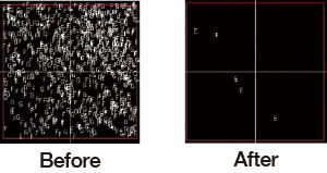
Application 2 : Patterned Reticle Inspection
PR-PD3 Pro
Detects particles on a wide range of mask and reticle. Enables high throughput with simple operation and 0.5 micron sensitivity.
Microscopes with multiple magnification are built in for particle observation and image data can be stored in the system.Valuable options are available, such as auto focus, auto sizing, etc. and data management functions are also available. Compact equipment design can save the installation space.
Features;
Multi surface inspection
Inspection of 3 surfaces within about 15 minutes*
Pattern surface 0.5 μm
Glass surface 5 μm
Pellicle surface 5 or 10 μm
* Load or Unload included
Sample case handling
SMIF box
Popular stepper case
Application 3 : Advanced Pellicle Inspection
PR-PD3EP
Detects particles on leading edge pellicle membranes enabling high throughput inspection of multiple membrane materials.
Auto defect image capture function
Automatically locates particles, captures images and saves to file
Auto defect sizing function
Automatically calculates size of particles based on captured images
Reticle edge handling
Complies with SEMI standard
Application 4 : Particle Removal
Automatically removes particles from wafers, reticles and pellicle surfaces with air / N blow and vacuum suction. Prevents the removed particles from re-adhering.
Reduction in running costs
Removal of particles by routine use extends both the replacement cycle of the pellicle and the cleaning cycle of the mask.
When particles on the glass surface are removed (OSL 5.0 μm)


