


")


Hayabusa2 Project

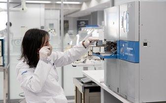
The HORIBA Group of worldwide companies provides an extensive array of instruments and systems for applications ranging from automotive R&D, process and environmental monitoring, in-vitro medical diagnostics, semiconductor manufacturing and metrology, to a broad range of scientific R&D and QC measurements. Proven quality and trustworthy performance have established widespread confidence in the HORIBA Brand.

Since establishing HORIBA RADIO LABORATORY in Japan in 1945, HORIBA has grown as an R&D company and engaged in international operations, making the most of its experiences and encounters with people along the way. We will continue to meet the varied needs of the world through our measurement and analysis technology.
Read more about HORIBA solutions and applications
The "Our Future" website serves as a special platform that highlights HORIBA Group's Vision, Mission, and Values. It outlines the entity HORIBA group aims to become and how we intend to contribute towards a healthier, sustainable, and better future.
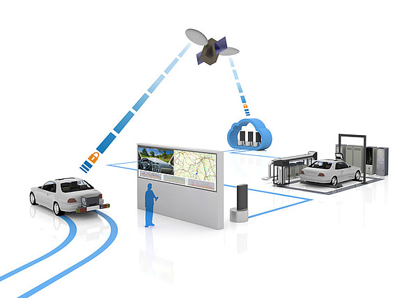
MoreRDE+ is a rapid, robust, integrated process and toolchain to deliver design, development, validation and verification with optimum efficiency.
MorePortable and Lab-based solutions for Agriculture Analysis & Crop Science
MoreWater sources such as rivers and lakes, which provide clean water,
are important elements that support people's lives.
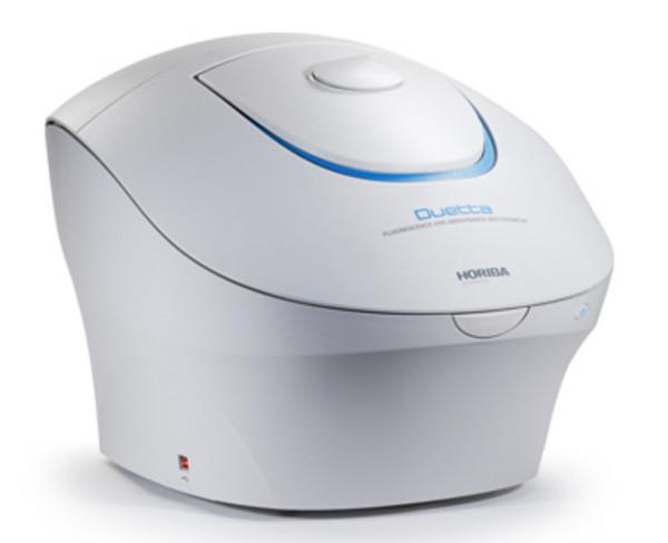
The Duetta simultaneously measures hundreds of fluorescence and absorbance spectra to deliver true molecular fingerprinting of your samples.
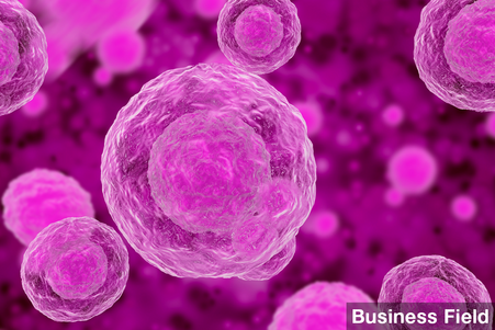
moreIn this issue of Chase the Case, we present a clinical case of Chronic Lymphoid Leukemia (CLL). The diagnosis was supported by the HORIBA Yumizen…
HORIBA Europe's David Schroeck, Global Product Manager Wind Tunnel Technologies, explains what and why a wind tunnel balance is essential...
Launch of HORIBA Group The “Our Future” (Vision, Mission, Values) dedicated website presents the HORIBA Group vision for the world and the kind of…
The latest issue of Chase the Case is from a patient diagnosed with Lymphocytosis. See how the hematology analyzer Yumizen H2500 shows the presence of…
The 44th edition of the QSP Blood Cell Morphology Newsletter features a case study and a quick overview of Nucleated Red Blood Cells (NRBC).
► Read…
HORIBA TECHNO SERVICE Co., Ltd. (hereinafter “HORIBA TECHNO SERVICE”), a Horiba Group company handling analysis/service businesses, joined the…
Let's review last month's blood slide cases in the latest QSP Newsletter, with a focus on AML cases in detail. Additionally, take our monthly cell…
Total immaturity of WBCs is of clinical importance to identify the morphologies and classify infections, inflammations, or hematology…
This year’s theme is ‘Analytical and Measurement Technologies for a Clean Water Environment and Sustainable Society.’
This webinar will cover the topics of quality assurance & end of line testing in fuel cell and electrolyzer series production.
April 30, 2024 at…
Join us for a webinar introducing HORIBA's all-new SA-9650 dynamic surface area analyzer. This innovative instrument utilizes flowing gas to…
HORIBA will exhibit at the 16th Optatec in May 2024 - the international trade fair for optical technologies, components and systems in Frankfurt.
In this talk, we discuss the topic of EV isolation with a focus on the most popular method of size exclusion chromatography and the challenges in…
Visit HORIBA Scientific at the 245th ECS Meeting