| General Spectrometer Specifications* | |
|---|---|
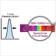
| Spectral Coverage | 185–1050 nm Tunable at factory between these ranges: 185-920 nm and 280-1050 nm |
| Spectral Resolution | 1.25 nm typical (22 μm slit width) and up, depending on the slit size |
| Spatial Resolution | 50 µm typical |
| Spectral Dispersion | 34.6 nm/mm; 0.38 nm/pixel |
| Focal Length | 116 mm |
| F/# | F/2.3 |
| Smile and Keystone | 1.5 pixel (typical) |
| Stray Light** | < 0.1% (typical) |
| Wavelength Accuracy | 0.1 nm (using multi-area wavelength calibration) |
| Software | LabVIEW™ acquisition software for initial evaluation (DLLs provided for software integration) |
| Specifications for Scientific Back-Illuminated CMOS Image Sensor with High Speed Electronics | ||
|---|---|---|
| Detector Model | sCMOS BI sensor with electronic rolling shutter (All the parameters are specified at normal room temperature of 25º C unless otherwise noted) | |
| Sensor Format*** | 2048 x 512 | |
| CMOS Pixel Size | 11 µm x 11 µm | |
| CMOS Height | 5.6 mm | |
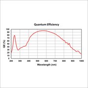
| CMOS QE | The peak QE is 77% at 250 nm and 95% at 560 nm (refer to graphs below) | |
| Thermoelectric Cooling | Uncooled | |
| Frame Rate | 94 fps (HDR mode), 188 fps (STD mode) on 2D sCMOS sensor | |
| Full Well | 80 ke¯ typical (HDR mode) | |
| Readout Noise | 1.6 e¯ typical, 2.0 e¯ maximum | |
| Digitization | 16-bit (HDR mode), 12-bit (High Sensitivity mode | |
| Dynamic Range (HDR mode) | 93.9 dB typical in HDR mode | |
| Non-linearity (measured on each system) | < 1.8% (maximum) in HDR mode | <0.9% (maximum) at high gain |
| Communication | USB 3 | |
| Environmental Conditions | Operating temperature 15° C to 40°C ambient; Relative humidity <70% (non-condensing); Storage temperature -25° C to 45° C | |
| Power requirements AC/DC Power Supply (provided) | 90-264 VAC, 47–63 Hz | |
* Specifications, form factor, and spectrometer cover subject to change without notice. No LabVIEW license is needed to run our acquisition software.
** Stray light using BP Filter: Baseline light level, outside the band, divided by BP peak (unsaturated) value.
*** See sensor manufacturer’s Blemish / Defect information
Scientific CMOS Back-Illuminated Sensor Quantum Efficiency

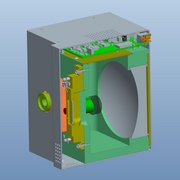
Mechanical Drawings

You can email OEM Technical Sales at: OEM.US(at)horiba.com or contact OEM at: +1.732.494.8660 Ext. 7733


