PDF
0.86
MB

Characterization of MoS2 Flakes
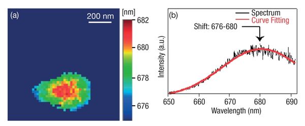
Both TEPL and TERS images are well correlated with AFM morphological images obtained simultaneously, and all are consistent in revealing the nature (number of layers) of MoS2 flakes. Upon deconvolution, the TEPL signal is even capable of revealing local inhomogeneities within a MoS2 flake of 100 nm size. Kelvin probe measurement supports TEPL and TERS measurements and adds to the power of such tip-enhanced combinative tools. TEOS characterization of 2D materials is likely to contribute to further deployment of these materials into commercial products through a better understanding of their electrical and chemical properties at the nanoscale.