<< Back to OEM Solutions for Semiconductors
In the semiconductor industry, where precision is critical, metrology plays a crucial role in quality assurance, process optimization, and overall yield improvement. As semiconductors become increasingly integral to fields like electronics, automotive, and artificial intelligence, the demand for sophisticated metrology techniques has surged.
Today's market reflects this shift, with a growing emphasis on advanced wafer inspection and analysis. From identifying surface imperfections and detecting particulate contamination, to ensuring structural uniformity at nanoscale resolutions, metrology enables the rigorous quality control required to meet the performance standards of modern devices.
In the semiconductor domain, Optical Emission Spectroscopy (OES) is valuable for monitoring and controlling plasma processes in real-time, which is essential for maintaining the purity and consistency of layers deposited on wafers.
HORIBA offers solutions specifically designed to address these complex demands. By integrating technologies such as reflectometry, multitrack spectroscopy, and hyperspectral and Raman spectrometry, HORIBA’s solutions empower semiconductor manufacturers to achieve unparalleled measurement precision and insight.
Wafer inspection by reflectometry | Raman wafer reader | Multitrack spectroscopy and hyperspectral imaging | HORIBA solutions
UV-VIS spectroscopic reflectometry is a vital non-contact, non-destructive optical technique used for inspecting semiconductor wafers. Inspection by reflectometry works by measuring the reflectance of specific wavelengths of light from the wafer’s surface, which allows for precise determination of layer thickness, uniformity, and defect detection.
This technique is essential in semiconductor manufacturing, as even microscopic inconsistencies or surface irregularities can significantly impact a device's performance, reliability, and longevity. Undetected defects can lead to significant downstream failures, resulting in higher production costs and potential delays, especially as these issues often become evident only in later manufacturing stages.
UV-VIS spectroscopic reflectometry systems are designed to mitigate these risks by offering high sensitivity, precision, and speed in measurement. These solutions provide accurate, reliable measurements with minimal downtime, allowing manufacturers to maintain quality standards and reduce waste. They can perform rapid, multi-point inspections across wafers, ensuring consistency and reliability throughout the production process.
A Raman wafer reader is an advanced tool that leverages Raman spectroscopy to characterize materials on semiconductor wafers. This non-destructive technique provides insights into molecular vibrations, allowing manufacturers to identify material composition, assess crystalline structure, and evaluate other critical properties that impact semiconductor quality.
Raman spectroscopy is especially valuable in semiconductor manufacturing for materials like graphene, which are increasingly used due to their exceptional electronic properties. This technique offers detailed information on the structural and electronic properties of graphene, as well as on the quality and uniformity of its layers across the wafer.
This analysis is crucial for quality control, as it allows manufacturers to detect inconsistencies in material properties that may compromise the performance and durability of semiconductor devices.
Multitrack spectroscopy allows simultaneous data collection from multiple points on a wafer, leveraging multichannel fiber optics. This method enables rapid, high-throughput analysis by capturing spectral data from various areas at once, providing a more comprehensive picture of the wafer’s properties and reducing the time required for inspection.
Hyperspectral imaging captures a broad spectrum of wavelengths for each point along an imaged line, creating a detailed spectral “fingerprint” at each location. When these spectral signatures are combined into an image, they produce highly informative maps that highlight variations in optical properties, material composition, and even potential defects.
Together, these techniques allow for precise mapping of a wafer's optical characteristics and identification of any inconsistencies or irregularities across the entire surface that could impact device performance and reliability.
These integrations allow for more accurate, reliable measurements, supporting both the high sensitivity of hyperspectral imaging and the rapid data collection of multitrack spectroscopy. They ensure that semiconductor manufacturers can trust their spectral data, helping maintain production consistency and meet the precision demands of today’s advanced semiconductor applications.
HORIBA’s advanced metrology solutions provide precise characterization of wafers, thin films, and device structures. Utilizing techniques like reflectometry, spectroscopy, and Raman analysis, our instruments ensure accurate process control, defect detection, and material analysis, optimizing yield and performance in semiconductor fabrication and R&D.

X선 분석 현미경 초대형 챔버 모델
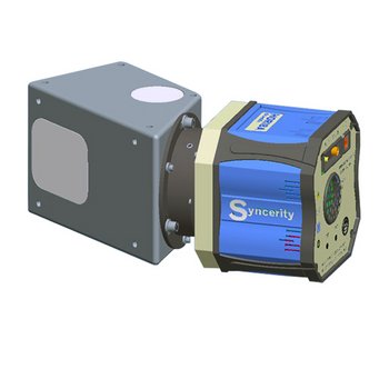
UV-VIS-NIR Spectrometer
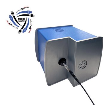
Multichannel Spectrometer and Hyperspectral Line Imager

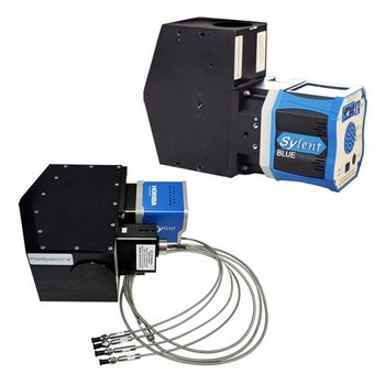
Miniature Multi Communication UV-NIR Spectrometer
HORIBA제품의 자세한 정보를 원하시면, 아래의 양식에 내용을 입력을 부탁드립니다.