Sie haben Fragen oder Wünsche? Nutzen Sie dieses Formular, um mit unseren Spezialisten in Kontakt zu treten.
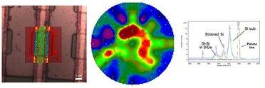
Photoluminescence and Raman Wafer Imaging
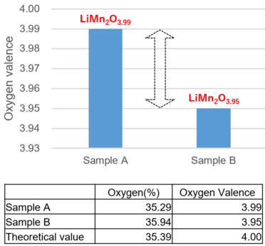
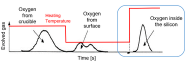
Oxygen/Nitrogen/Hydrogen Analyzer
(Flagship High-Accuracy Model)
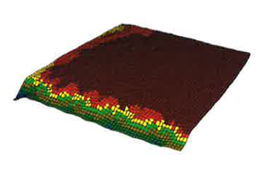
Real-time and Direct Correlative Nanoscopy
Oxygen/Nitrogen Analyzer (Entry Model)
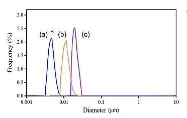
Centrifugal Nanoparticle Analyzer
Raman Photoluminescence & Cathodoluminescence
Discover a Whole New World of Information with Glow Discharge Optical Emission Spectrometer
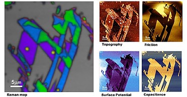
AFM-Raman for physical and chemical imaging
Oxygen/Nitrogen Analyzer
AFM-Raman for Physical and Chemical imaging
Versatile AFM Optical Coupling
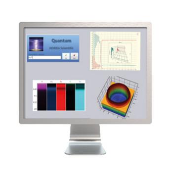
Quantum and Image
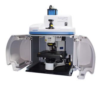
Confocal Raman Microscope
Oxygen/Nitrogen/Hydrogen Analyzer
Versatile Hyperspectral Cathodoluminescence
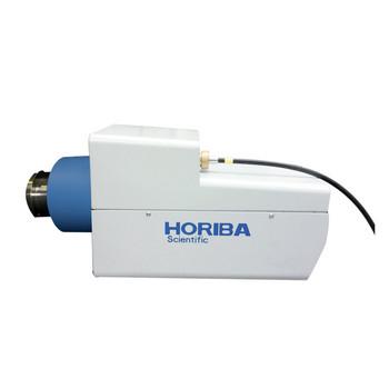
MicroRaman Spectrometer - Confocal Raman Microscope
Confocal Raman & High-Resolution Spectrometer
Compact Hyperspectral Cathodoluminescence
Ultra-Fast, Sensitive and High Resolution Depth Profiling technique
Highly sensitive silica monitor for ultra-pure water management in semiconductor/FPD processes
Fast Imaging Cathodoluminescence
The AFM optical platform
Powerful and Cost Effective Spectroscopic Ellipsometer
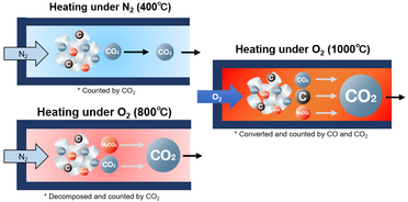
Carbon/Sulfur Analyzer (Tubular Electric Resistance Heating Furnace Model)
Spectroscopic Ellipsometer for Simple Thin Film Measurement
Cathodoluminescence Solutions for Electron Microscopy
Spectroscopic Ellipsometer from FUV to NIR: 190 to 2100 nm
A versatile spectroscopic ellipsometer covering a large range from VUV to NIR
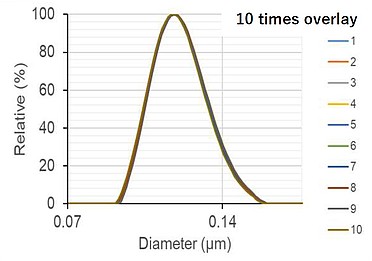
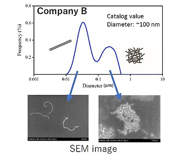
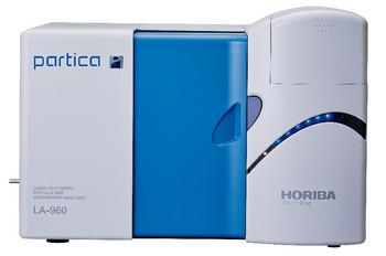
Laser Scattering Particle Size Distribution Analyzer
Micro Volume pH Monitor
Laser Scattering Particle Size Distribution Analyzer
Resistivity Meter for Semiconductor Cleaning Processes
Industrial pH meter
Stand-alone Type Chemical Concentration Monitor
Carbon Sensor Conductivity Meter (High concentration type)
Carbon Sensor Conductivity Meter (Low concentration type)
2-Channel Resistivity Meter
High Precision, High Stability Chemical Concentration Monitor


")


")
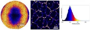
 Raman map of MoS2 layers.")
 and C70 (b) fullerenes.")


")

,HE-960LC")

")
