Advanced material characterization using multimodal spectroscopy is essential to realizing the full potential of wide-bandgap (WBG) semiconductors like silicon carbide (SiC) and gallium nitride (GaN). Techniques including Raman spectroscopy, photoluminescence (PL), and ellipsometry are required to detect critical manufacturing issues such as residual stress, contamination, and crystal defects. Synergizing these techniques through advanced correlative platforms ensures high wafer uniformity, prevents device failure, and maximizes manufacturing yield.
Read the full article at:
https://www.photonics.com/Articles/Multimodal-Spectroscopy-Optimizes-High-Yield/p5/a72143
Wide-bandgap (WBG) semiconductors, such as silicon carbide (SiC) and gallium nitride (GaN), feature energy gaps greater than 2 eV to enable extreme power and high-frequency applications. Addressing the critical pain point of thermal failure in standard silicon, these advanced materials provide exceptional thermal conductivity and high breakdown voltages. This allows manufacturers to build robust, highly efficient power electronics and powertrains for electric vehicles.
The primary hurdle in high-quality wafer fabrication is managing residual stress and crystal defects that drastically degrade device efficiency. High-temperature processing steps introduce severe thermal gradients, leading to mechanical warping, micropipes, and line dislocations. Furthermore, trace metallic contamination causes problematic doping variations and unpredictable electrical behavior, requiring precise optical characterization to ensure absolute wafer uniformity and maximize manufacturing yields.
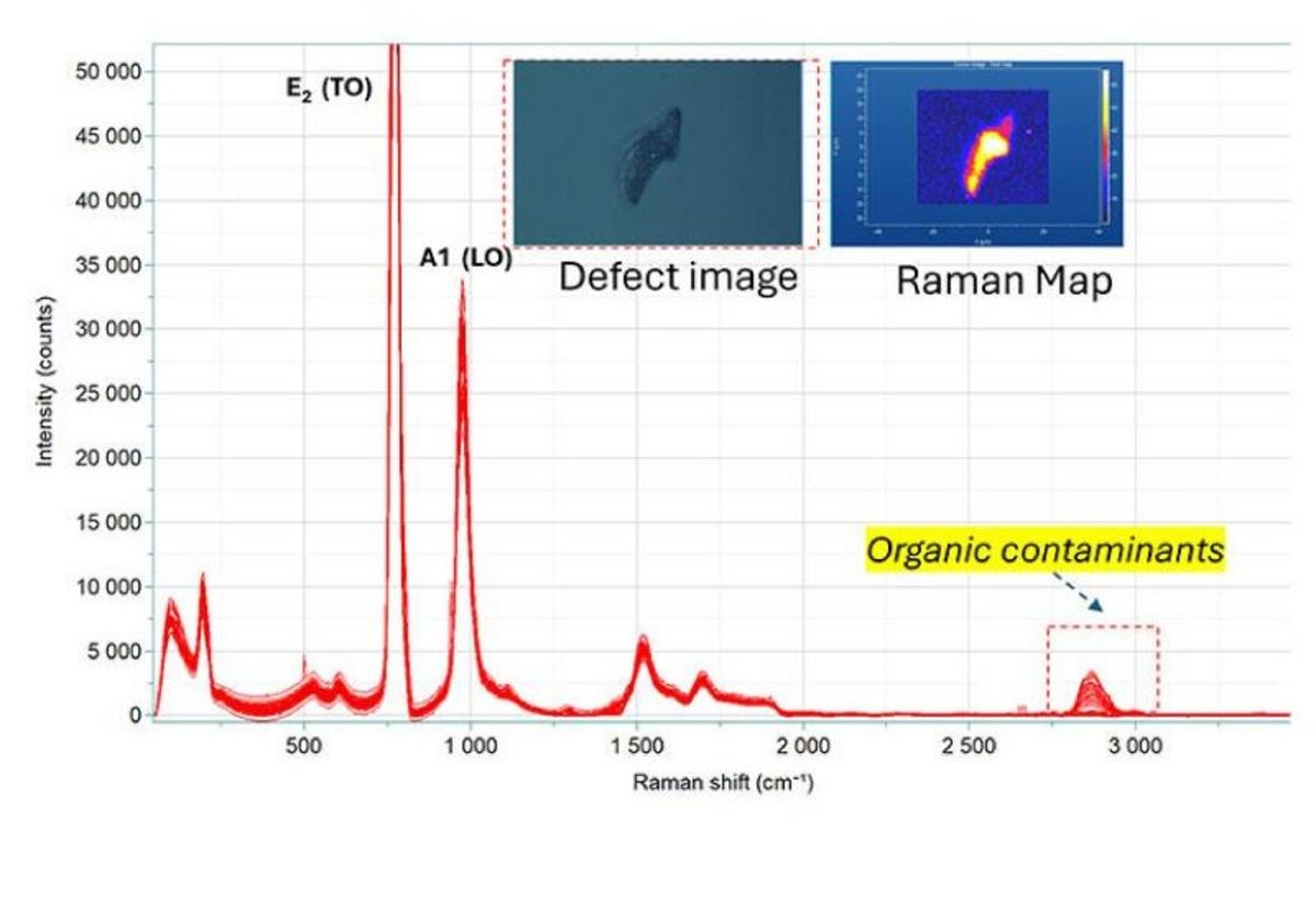
Raman spectroscopy maps residual stress and identifies localized surface contamination by probing the inherent vibrational modes of the crystal lattice. By analyzing subtle shifts in Raman bands, engineers determine the exact magnitude and spatial distribution of internal strain across the wafer. Beyond mapping structural strain, this non-destructive technique measures crystal linewidth to accurately calculate overall defect density.
Deep-ultraviolet (DUV) excitation drives photoluminescence (PL) and cathodoluminescence (CL) to effectively identify point defects, dislocations, and impurities in WBG materials. Because SiC and GaN possess substantial energy gaps, high-energy photons are required for efficient probing. These targeted luminescence spectroscopies map carrier lifetimes and provide depth-sensitive analysis of localized energy states, immediately identifying non-radiative recombination centers that reduce overall device performance.
A synergistic multimodal analysis approach combines the strengths of various spectroscopic methods to provide a comprehensive understanding of complex wafer quality. For example, engineers correlate wafer-level stress maps from Raman scattering with sub-micron defect visualizations from differential interference contrast (DIC) microscopy. This complete correlation between fundamental material science and automated inspection accurately predicts device performance and optimizes high-volume production operations.
Tiene alguna pregunta o solicitud? Utilice este formulario para ponerse en contacto con nuestros especialistas.