
Glow Discharge Optical Emission Spectrometry (GD OES) is an Ultra-Fast Elemental Depth Profiling Technique used for Process Optimization and Process Control in LED and thin films PV manufacturing to control the deposition of multilayered structures using a large number of materials (GaN or GaAs for LED, perovskites, tandem or CIGS for PV), with dopants but also contaminants.
Thin & Thick Films can be probed in seconds to minutes with excellent depth resolution using a pulsed RF plasma that will sputter in depth a representative area of the material investigated. The technique is also central in an analytical platform as fast access to clean embedded interfaces for complementary measurements by XPS, SEM, Ellipsometry, PL, micro Raman is provided.
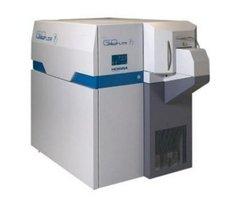 | |
| Instrument | GD Profiler 2 |
| Elements | All possible (selection depending on application) |
| Etching Rate | Several nm per socond |
| Depth resolution | nm |
HORIBA제품의 자세한 정보를 원하시면, 아래의 양식에 내용을 입력을 부탁드립니다.